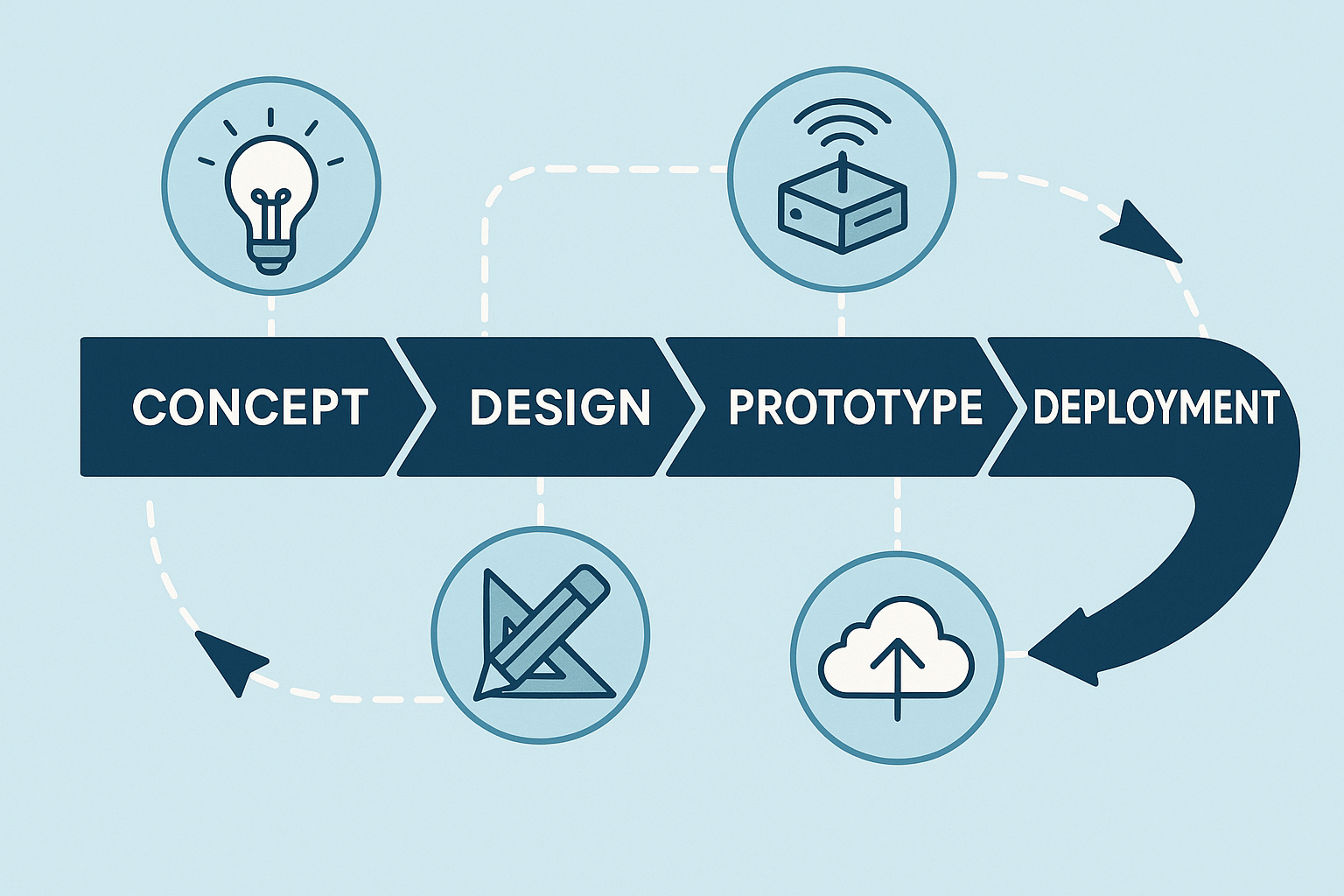
So you’ve got an idea for the next big IoT gadget? Awesome! Before you dive into coding, soldering, or ordering a truckload of circuit boards, let’s take a step back. Developing a cloud-connected IoT sensing product from scratch is quite a journey. This introduction will walk you through a field-tested, end-to-end playbook for bringing an embedded IoT product from the spark of an idea all the way to a successful launch. We’ll keep it light, fun, and easy to follow – professional with a dash of humor – because even serious engineering can have its moments of fun. Whether you’re a rookie product manager, a budding engineer, or an aspiring architect, this guide will give you a bird’s-eye view of the process and what to expect at each stage.
Why follow a playbook? Well, IoT projects involve many moving parts: hardware, firmware, cloud services, apps, you name it. It’s like juggling multiple balls (or chainsaws!) – without a plan, you might drop one. This playbook combines the best of classical systems engineering (to make sure we don’t miss anything critical) with an Agile, iterative cadence (so our firmware and cloud software teams can move fast and adapt). In plain English: we’ll be structured but not rigid. Now, let’s break down the journey into clear stages, from Stage 0 (yes, we start counting at zero, because engineers 😉) through Stage 8, and beyond. Buckle up and let’s get started on turning that IoT idea into reality!
Stage 0: Concept & Feasibility (“Why are we doing this?”)
Every great project begins with why. Stage 0 is all about clarifying the purpose of your idea. In this Concept & Feasibility stage, we figure out why this product should exist and if it makes sense to pursue it. Think of it as a reality check for your idea before you start investing serious time and money.
- Goal: Pin down the business or research need for your product. What problem does it solve? Who would care? If you can’t answer these clearly, now’s the time to figure it out.
- Typical Outputs: At this stage, you’ll likely craft a short vision statement (a clear, inspiring sentence or two about what you’re building and why). You might sketch out some high-level user journeys – basically, simple stories of how a user would interact with your device (“Alice installs the sensor in her greenhouse, and it alerts her smartphone if the temperature goes out of range”). You’ll also want to do a rough market analysis or ROI estimate. Is there a market for this gadget? Would it save money or improve lives enough that people want it? This doesn’t need to be a 50-page thesis – just enough research to give confidence (or reveal red flags).
- Tip: Do this quickly – in days, not weeks. The idea is to validate or kill the idea early. If your concept has a fatal flaw (no market demand, insanely high cost, etc.), it’s far better to discover that before you’ve spent months designing a prototype. Think of Stage 0 as a filter: it catches the bad ideas so you don’t waste resources, and it lets the promising ones through. Be brutally honest with yourself here; it’s like the preliminary audition before the big show. If something doesn’t look viable, it’s okay to shelve it and move on to the next idea.
By the end of Stage 0, you should have a clear answer to “Why are we doing this?” and confidence that the idea is worth pursuing. If you do, congrats – you’ve got the green light to move forward! 🎉 And if not, don’t be discouraged; better to fail fast at the idea stage than later when the stakes (and costs) are higher.
Stage 1: Stakeholder & System Requirements (First things first!)
Alright, you’ve decided the idea is a keeper. What’s next? Requirements – always requirements first. This might not sound as exciting as building stuff, but trust us, it’s the foundation for everything to come. Think of Stage 1 as drawing the treasure map before you set sail. Skipping this step is like embarking on a voyage with no map – adventurous, perhaps, but likely to end poorly. 😅
What are “requirements”? Essentially, they’re a detailed list of what the product must do and under what conditions. This includes different categories of requirements:
- Functional Requirements: These describe what the product does. For an IoT sensor, functional requirements might cover what data is sensed (e.g. temperature, humidity), with what accuracy, how often readings are taken (update rate), and how quickly data must be delivered (latency). It answers questions like: What features will the product have? What tasks should it perform? For example, “The device shall measure temperature from 0°C to 50°C with ±0.5°C accuracy and send readings to the cloud every 10 minutes.”
- Non-Functional Requirements: These cover the constraints and qualities of the product – things like power consumption (e.g. must run on battery for at least 1 year), reliability and longevity (Mean Time Between Failures, aka MTBF, maybe it needs to run for 5 years without crashing), security/privacy considerations (data must be encrypted, user data must be protected), cost limits (unit cost should not exceed $50), and any regulatory standards it must meet (for example, compliance with CE or FCC rules for electronics, or a safety standard like ISO 13849 if it’s used in machinery). Non-functional requirements are just as critical as the flashy features; they ensure the product is safe, robust, and viable in the real world.
- Interface Requirements: These define how your product will interact with the outside world. This includes electrical interfaces (e.g. does it output a 0-5V signal to another device? does it use USB-C for power?), mechanical interfaces (the physical dimensions, mounting points, connectors – will it fit in a certain enclosure or slot? does it need to be waterproof?), and communication interfaces like cloud APIs or mobile apps (e.g. “The device shall provide a REST API endpoint for retrieving sensor data” or “It shall connect via BLE to a smartphone app”). Basically, how will all the pieces (device, cloud, app, other systems) plug together and talk to each other?
How do we capture these requirements? In practice, you might write a formal requirements document or keep a structured list in a project management tool. Some teams use an IEEE 29148-based template for System Requirements (which is a fancy standardized format for writing requirements – great for thoroughness). Others use a more agile approach, like a list of epics and user stories in Jira or a wiki. Whichever format you choose, make sure each requirement is clear and testable. A good habit is to tag each requirement with how you’ll verify it later – will it be verified by test, by inspection, by analysis, or by some certification? For example, if you have a requirement “Device shall have an IP67 waterproof rating,” you know later you’ll need to do a water ingress test to verify it.
Now, why insist on doing this first? Because every later design, test, and compliance check will trace back to these requirements. They are the North Star for your project. If you charge ahead into design without solid requirements, you might build the wrong thing, or miss something crucial (imagine designing a beautiful device and then someone says, “Actually, it also needed to measure humidity,” and you have no space left on your PCB for that sensor – oops!). It’s much cheaper and easier to change or clarify requirements now than to rewrite firmware or reroute a PCB later.
A bit of humor to remember this stage: Changing your mind on a requirement later is like deciding to add an extra bedroom after your house is built – it’s possible, but painful and expensive. So, get those requirements right early on. Engage all your stakeholders (marketing, engineering, customers, etc.) to make sure nothing critical is missed. As a result, you’ll have a clear blueprint for what the product must achieve, which guides everyone (hardware engineers, software developers, testers, etc.) in the next stages.
Stage 2: System Architecture (Plan on Paper Before You Build)
With solid requirements in hand, it’s time for the System Architecture – essentially, the high-level game plan for how you’ll meet those requirements. Think of architecture as the design of a city before you start constructing buildings. You decide where the roads and bridges go before pouring concrete. In our IoT project, this means sketching out the overall system on paper or a whiteboard (digital “paper” is fine too) before any soldering or coding happens. This stage is all about big-picture thinking and making the key decisions that will shape your product’s design.
Here’s what happens in system architecture:
- Block Diagram of the Whole System: You draw out all the major components and how they connect. For example, a simple block diagram might be:
Sensor → Microcontroller (MCU/SoC) → Wireless Radio → Cloud Server → Web/Mobile Client.
This shows the end-to-end path: the sensor feeds data to the MCU, which might do some processing and then uses a radio (like Wi-Fi, Bluetooth, or LoRa, etc.) to send data to a server in the cloud, which then makes it available to a user interface (web dashboard or mobile app). By having this diagram, everyone can see all the pieces involved at a glance. - Partitioning Decisions: Now that you see the pieces, decide which responsibilities live where. This is about dividing tasks between hardware, firmware, and cloud. For example, will you handle data encryption on the device (so data is secure before it even leaves the sensor box), or will you do it in the cloud? Should the sensor data be pre-processed on the device (e.g. filtering or averaging) or just sent raw to the cloud where heavy computing can happen? These decisions impact hardware requirements (do you need a more powerful MCU for on-device processing?) and software complexity (cloud might be simpler if device does more, or vice versa). It’s a bit of a balancing act – you want each part of the system to handle what it’s best at. Often you’ll iterate on these choices: maybe initially you plan to do everything on a tiny MCU, but then realize memory is too limited, so you shift some functionality to the cloud, etc. That’s exactly the kind of insight you want to have now, in the architecture stage, rather than later when you’ve already written code or made a PCB that can’t handle it.
- Technology Selection: Based on requirements and your block diagram, start picking candidate technologies for each part. This is where you choose, for instance, which sensor(s) to use (do you need a high-precision digital sensor or something analog with an ADC?), what MCU or SoC family might fit (does it need to be ultra-low-power? high-speed? lots of RAM? any specific vendor platform you prefer?), and what connectivity method suits your use case (Bluetooth Low Energy for short-range and phone connectivity, Wi-Fi if there’s local internet, LTE-M/NB-IoT if it needs cellular, LoRa if long-range low-bandwidth is key, etc.). You don’t necessarily finalize the exact part numbers yet, but you narrow it down (e.g. “We’ll probably use an ARM Cortex-M4 MCU, with a Semtech LoRa radio”). Also think of things like power: will it run on battery, and if so what kind (coin cell vs. Li-ion)? If it’s battery-powered, that immediately rules out some high-power tech. Essentially, you’re shaping the tech stack for the project here.
- Risk & Cost Analysis: Even at this early stage, identify potential risks or cost drivers. Does your design rely on a single component that’s expensive or has a 30-week lead time? (In hardware, that’s a real concern – sometimes a chip is perfect but always out of stock 😫.) Are there any “single points of failure” in your system? (For example, if the device loses cloud connection, does the whole product become useless? Maybe you need some local storage as backup.) Also consider certification or compliance challenges: e.g. using a certain wireless frequency might entail complicated certification. By flagging these now, you can plan mitigations – maybe have a backup component in mind, or plan extra time for certification testing, etc. It’s much better to walk in with eyes open to the big risks than to be surprised later.
- Documentation & Notation: You’ll want to capture the architecture in a way that’s understandable and shareable. Many teams use visual modeling languages: SysML or a simple C4 model for system context diagrams can show the cross-discipline view (hardware, software, users, all interacting). For the software elements (firmware and cloud), a UML component diagram can illustrate how the software parts are split (e.g. which pieces run on the device vs on the server). But don’t worry if those acronyms sound intimidating – even hand-drawn boxes-and-arrows or a PowerPoint slide can do the job, as long as it’s clear. Some people also start a basic Bill of Materials (BOM) in a spreadsheet at this point, listing key components (sensor, MCU, radio module, etc.) with rough costs and any notes (like lead times or vendor). This helps ensure the product can hit its cost targets and that you’re aware of any sourcing challenges early.
The mantra for Stage 2 is “design twice, build once.” By hashing out the system architecture on paper first, you save yourself from expensive do-overs later. It’s a lot cheaper to move boxes and arrows in a diagram than to move traces on a fabricated PCB or rewrite a codebase. Plus, it gets all your team members (hardware, firmware, cloud, product, etc.) on the same page early. Everyone can provide input: maybe the cloud engineer says “hey, if the device could tag data with a timestamp, it’d simplify my part,” or the hardware engineer says “if we had two sensors instead of one, we could also measure X.” These discussions are invaluable before everything is set in stone.
Finally, by the end of Stage 2, you should have a clear blueprint: a top-level design that shows how you intend to meet the requirements. It’s like the architectural drawing of a building – you’re not deciding the color of the paint yet, but you know how many floors it’ll have and where the doors and windows will be. With that blueprint ready, you’re prepared to dive into detailed design with confidence.
Stage 3: Electronics & Mechanical Design (the “Left-Hand Side” of the V)
Now we’re getting to the hands-on fun: designing the actual hardware! Stage 3 covers electronics and mechanical design, which often go hand-in-hand. If you’ve heard of the V-model in engineering (a classic development process model), the “left side” of the V is all about design and implementation. That’s where we are now – designing the hardware that will later be verified and validated on the right side of the V. But don’t worry if you’re not familiar with the term; the key idea is that hardware design is more sequential and must be done with care, because once you print a circuit board or mold a plastic case, changes are a bit tricky (read: expensive 😬).
Stage 3 can be broken into a few sub-steps, and importantly, this is where hardware and software development start working in parallel (more on the software in the next stage). Here’s how the hardware side typically unfolds:
- Schematic Capture: This is where the electrical circuit design is drawn out in detail. Using CAD tools (like Altium, Eagle, KiCad, etc.), the electronics engineer creates a schematic: basically an electronic diagram showing all components (microcontroller, sensors, capacitors, connectors, etc.) and how they’re connected with nets (wires). Once the schematic is ready, it’s critical to do a review – often a PDF of the schematic is circulated for peers to catch mistakes (like “Oops, the sensor’s power pin isn’t connected!” or “That resistor value seems off”). At this stage, some teams also conduct an FMEA (Failure Modes and Effects Analysis) especially for crucial circuits like the power supply or any safety-related parts. FMEA is a fancy way of saying “think of all the ways this could fail and ensure we have mitigations or the risk is acceptable.” For example, what if the temperature sensor fails short-circuit? Will it damage the board or just return a max reading? Addressing such questions early improves reliability. Meanwhile – and this is key – in parallel a bit of software work can start. The firmware team can begin creating a HAL (Hardware Abstraction Layer) skeleton based on the schematic. Essentially, they prepare software interfaces for the microcontroller peripherals (like I2C or SPI drivers if those sensors use those buses) and they can even write unit tests for these on a PC (without hardware). This parallel effort means the software folks aren’t twiddling their thumbs waiting for boards; they’re laying groundwork that will make bringing up the hardware easier later.
- PCB Layout: Once the schematic is finalized, it’s PCB (Printed Circuit Board) time. The PCB layout is where you place all those components onto a board shape and route the copper traces to connect everything, again using CAD software. This stage produces outputs like Gerber files (the files needed by manufacturers to actually fabricate the board) and often a 3D model (STEP file) of the board, which is super helpful for mechanical integration (checking that the board fits in the enclosure, etc.). During PCB layout, you also keep in mind Design for Manufacturing (DFM) and Design for Test (DFT) guidelines – basically making sure your board can be manufactured reliably and that you can test it easily later. For instance, you’d want to add test pads or connectors for programming the firmware and testing signals on the board. A checklist is often used to not forget things like fiducials (for pick-and-place machines), clearances, labelling, etc. While the board is being laid out, the software team can progress in parallel: they can simulate or stub out sensor drivers (if they know the sensor model from the schematic, they might write code against a datasheet or use a sensor emulator). The cloud team might set up a skeleton of the backend (maybe design the database schema for sensor data, or set up a basic server that can accept a data point). These parallel tasks ensure that by the time hardware arrives, the firmware and cloud are not starting from zero – they’re ready to integrate.
- Prototype Build: With PCB layout done, you send those Gerbers out to a fab (many use quick-turn PCB manufacturers) and order parts (if you haven’t already). Pro Tip: Order critical parts as soon as your schematic/footprint is certain! Some parts can have long lead times (a lesson many learned the hard way during chip shortages). Order early so by the time boards arrive, you actually have the chips to put on them. Once the boards and parts are in, you assemble a few prototype units – this could be in-house if you have a lab and steady soldering hands, or via an assembly service. Now the exciting moment: bring-up of the first board. This involves powering it on (often with fingers crossed and a current-limited power supply… just in case) and verifying that the basics work. Does the MCU turn on and run code? Are the power rails at the correct voltages? Can you communicate with the sensor over I2C/SPI, etc.? Often you’ll connect a debugger or serial console to see if the firmware is alive (even blinking an LED or printing “Hello” is a big win at this stage!). You also check for any power or thermal issues – e.g. nothing is overheating or drawing more power than expected. If you planned for regulatory compliance (say FCC emission tests), you might do a pre-scan at a lab just to see if you’re in the ballpark or if something is screaming at an unexpected frequency. During prototype bring-up, the firmware team is now testing their code on real hardware – writing those sensor drivers for real, tuning the RTOS tasks (if an RTOS is used), and so on. The cloud team might start seeing real data come through and verify the end-to-end flow on a small scale.
Stage 3 often involves a few iterations: you might find a mistake on the board and have to bodge-wire a fix or spin a revision. That’s normal! This is why we build prototypes – to learn and improve. Close collaboration between hardware and software here is vital; as issues come up, the teams work together to troubleshoot. For example, if the sensor isn’t reading, is it a firmware bug or a wiring issue? Both sides investigate.
Throughout all this, keep in mind DFM (Design for Manufacturing) if you plan to mass-produce, and DFT (Design for Test) to ensure you can efficiently test units in production. It’s easier to add a test connector or programming header now than to figure out how to test 1,000 units later with no easy access to signals.
By the end of Stage 3, you should have working prototype devices and a lot of lessons learned. You’ll have initial data on performance (power consumption, sensor accuracy in real conditions, etc.), and maybe a list of fixes for the next version. But importantly, you’ve built the physical foundation of your IoT product. 🎉
Side note humor: The first time a prototype comes to life and sends data to the screen, it’s okay to feel a bit like Dr. Frankenstein yelling “It’s alive!” – we all do a little happy dance at bring-up success. Just maybe don’t literally shout it in the lab; it scares the interns.
Stage 4: Firmware & Cloud Software Development (Iterative “Right-Hand V”)
While the hardware design was the left side of the V, Stage 4 is the right side – developing the firmware (the software that runs on the device) and the cloud software (servers, databases, APIs, user interfaces). This stage is typically much more iterative and runs in parallel to hardware development. In fact, you likely already started some firmware work back in Stage 3 (during schematic/layout). Now it ramps up fully. The key approach here is to use modern software development practices so you can build, test, and refine quickly – unlike hardware, software is easy to change on the fly, so we take advantage of that agility.
Stage 4 can be thought of in two parts: architecture/design for software, and the ongoing sprint cycle of development.
4.1 Software Architecture & Design
Before everyone jumps into coding like crazy, it’s wise to sketch out the software architecture for both the firmware and the cloud components. This is analogous to the system architecture we did in Stage 2, but at the code level. Key things to establish:
- Firmware Architecture: Define the layers and components of your embedded code. A common approach is layered architecture: for example, at the bottom you have a Board Support Package (BSP) or low-level drivers (for the MCU, peripherals, etc.), above that you have a hardware abstraction layer and device drivers for sensors/actuators, above that maybe a services layer (like communication services, data processing algorithms), and at the top the application logic (the code that ties it all together according to your product’s purpose). You might draw a simple diagram (UML package diagram or just boxes) showing these layers. Also consider the use of an RTOS (Real-Time Operating System) if your device has multiple tasks (like reading sensors, sending data, updating LEDs, etc. concurrently). If using an RTOS, part of the architecture design is deciding the task structure (e.g. one task for sensor sampling, one for communications, one for housekeeping, etc.) and how they communicate (message queues, shared data guarded by mutexes, etc.). Designing this clearly will help avoid the dreaded “spaghetti code” monster and make the firmware easier to maintain.
- Cloud Architecture: Similar thinking goes on for the cloud side. If you have a web server or IoT platform receiving data, sketch out its components. For instance, there might be an API layer (ingesting device data and handling user requests), a database (storing sensor readings, user info, etc.), and maybe some processing or analytics services (like triggering alerts if data goes out of range, etc.). Also consider the client side: perhaps a web app or mobile app that fetches data from the cloud. You could use a C4 model diagram at the Container level to show how the pieces (device, server, database, client app) interact. The goal is to have a clear mental model (and maybe a visual one) of the software ecosystem.
- Communication Protocols & Data Formats: Part of design is agreeing on how the device talks to the cloud. Will you use MQTT? HTTP/REST API? CoAP? Decide on the protocol and design the data format (e.g. JSON payloads with certain fields, or a binary format if you need efficiency). This might involve sequence diagrams – for example, sequence diagrams can illustrate how a sensor reading is taken on the device, packaged, sent to the cloud, acknowledged, and then shown to the user. This ensures both firmware and cloud engineers are literally “on the same page” about the message flow.
- Coding Standards and Tools: As a team, agree on how you’ll write code. For embedded C, many teams adopt MISRA-C guidelines (a set of rules to avoid troublesome C constructs). For C++ maybe the C++ Core Guidelines or a subset of modern C++ features that are safe for embedded. For Python (if doing cloud or scripting), PEP 8 style guide, etc. The idea is to keep code consistent and avoid common pitfalls. Also choose tools: version control (very likely Git), issue tracking, and CI (Continuous Integration) platform setup should be decided. This might seem procedural, but it’s important – it’s much easier to enforce code quality when everyone agrees on the rules from the start.
In short, Stage 4.1 is about planning the software just enough so that everyone knows the boundaries and interfaces. It’s like planning a road trip: you mark the route and stops, but you don’t necessarily script every single minute – there’s room for iteration once on the road.
4.2 Development Sprints (Iterate and Conquer)
Now the fun begins in earnest: writing code, testing it, and showing it works – in repeating cycles. This is often done in sprints (commonly 2 to 4 weeks long). The idea of a sprint is to take a set of features (user stories) from the backlog (which was informed by the requirements in Stage 1) and implement them, producing a potentially shippable increment of the product at the end of the sprint. Let’s break down what this looks like:
- Sprint Planning & User Stories: The team looks at the prioritized backlog and pulls in some user stories or tasks into the sprint. For example, a story might be “As a user, I want the device to send temperature data to the cloud every 10 minutes.” During planning, the devs clarify the acceptance criteria (e.g. what does “send to cloud” entail exactly? how will we know it’s working?).
- Implementation & Continuous Integration: During the sprint, developers write code for the firmware and cloud features. They also write automated tests for that code. A best practice is to use Continuous Integration (CI) – a system like GitHub Actions, GitLab CI, Jenkins, etc., that automatically builds the code and runs tests every time you push changes. For firmware, this might include running unit tests on a host machine or even on a hardware-in-the-loop setup (where a real device or a simulator is used in testing). For cloud, this definitely includes running all the server/app tests. The idea is to catch bugs quickly. Teams often also integrate static analysis tools (which scan the code for bugs or stylistic issues) and measure code coverage (to ensure tests are hitting most of the code). For instance, you might enforce that, say, at least 80% of your code is exercised by tests, and zero critical static analysis warnings are allowed.
- Incremental Builds: By the end of each sprint, you aim to have an incremental build of the whole system – a version of firmware that can be flashed onto a device and a version of the cloud software (maybe deployed in a test environment or as Docker containers) that work together. For example, at the end of Sprint 1, perhaps you have a basic end-to-end flow: the device reads a dummy sensor value and successfully sends it to the cloud, and you can see it in a simple database viewer. By Sprint 2, maybe it’s reading from the real sensor and you have a basic web dashboard showing one point. By Sprint N, you have all the features implemented. The key is iterative progress – each cycle adds more functionality and fixes.
- Testing and Done Criteria: Each user story or feature is considered “done” only when certain criteria are met. A common Definition of Done checklist might include:
- Code for the feature is written and builds without errors.
- Unit tests covering the new code are passing (and perhaps new tests are written if needed).
- Integration tests (if the feature interacts with other parts) are passing – e.g. if you added a cloud API, a test that calls that API and expects a correct response should pass.
- Static analysis shows no new warnings (and ideally no old ones either).
- The code has been peer reviewed (another developer looked at it and approved).
- Documentation is updated if needed (this could be as simple as updating a README or as formal as updating interface docs or diagrams if the architecture evolved).
- You have demoed the feature to the team or stakeholders to prove it works end-to-end.
- Continuous Documentation: One particularly cool tip some teams use: keep those architecture diagrams (from Stage 4.1) in sync with the code. If you use “diagrams as code” (like PlantUML or Mermaid), you can store the diagram source in your repository and even update it whenever things change. For example, if the design shifts (maybe you add a new microservice in the cloud or a new sensor on the device), update the diagram and regenerate it. Some CI setups even fail the build if you changed code that impacts architecture but didn’t update the diagrams. This way your documentation is always current. No more outdated wiki pages describing a version of the system that no longer exists!
- Regular Demos: At the end of each sprint (or even each week), it’s great to have a quick demo. Show the team (and other stakeholders) what’s working. “Look, the device is now sending data and we can see it on this dashboard!” These demos create a sense of progress and also enforce integration discipline – you can’t demo something unless the pieces actually work together. It’s amazing how motivating it can be to always have something to show, even if small. It also flushes out integration issues early (better to discover a mismatch between firmware and cloud in week 4 than in week 14).
To summarize Stage 4: It’s all about iterative development and continuous testing. By the end of it (likely after several sprints), you should have a firmware that is feature-complete and tested, and a cloud system that is feature-complete and tested – basically the full software side of your product ready to roll. Importantly, thanks to iterative working, you’ll have had many opportunities to adjust and improve along the way, rather than betting it all on one big bang integration at the end. This reduces risk and makes development more predictable (and frankly, more fun – because you see your product coming to life step by step 🎉).
Stage 5: Integration Gates (Making Sure it All Plays Nice Together)
By now, you have hardware prototypes (Stage 3) and iterative software builds (Stage 4). Stage 5 is about integrating everything and verifying at key milestones that the system is working end-to-end. We call these milestones Integration Gates – think of them as “checkpoint bosses” in a video game. You don’t move to the next level until you’ve proven certain capabilities at each gate. It’s a mix of excitement and anxiety as you combine hardware + firmware + cloud and watch for sparks (hopefully metaphorical ones only!).
Here are typical integration gates in an IoT product project:
- Bring-Up Gate: This is the first basic integration test with actual hardware. The goal at this gate is pretty humble: Does the MCU on our board boot up and run code? You’d verify that you can flash the firmware onto the device, that it starts executing (for example, a simple blinking LED or serial message like “Hello, world” confirms life). Also, check that the device can do rudimentary things like read its own battery level or supply voltage, and communicate with a debug console or logger. Essentially, the patient is alive. 🩺 This gate is passed when you have confirmed the board is not a brick and your fundamental hardware (power, clock, basic I/O) and toolchain (programmer, etc.) are working.
- Data-Path Gate: Now we test the core reason this whole system exists: getting sensor data from the device to the cloud. At the data-path gate, you should demonstrate that sensor values appear in the cloud database or server as expected. For example, if it’s a temperature sensor, you trigger some readings on the device, they get transmitted over the network (be it BLE, Wi-Fi, cellular, etc.), and end up in your cloud storage or application. You’ll check that the data is making the journey intact and timely – the readings have the correct timestamp, they’re within expected ranges and precision, and the update rate (say every 10 minutes) is being met. It’s essentially a full vertical slice of functionality: sensor -> device -> network -> cloud -> database. Passing this gate usually means the end-to-end data pipeline works in practice, not just theory. It’s a huge milestone because it proves your architecture and implementation deliver the fundamental value (collecting and transmitting data).
- User-Story Gate: Here we go one step further to what a real end user would experience. It’s not enough that data reaches a database; can a user actually benefit from it? At the User-Story gate, you integrate the front-end (like a mobile app or web dashboard) and show a real user-facing scenario working. For instance, a user opens the app and sees the live temperature reading from the device, maybe along with a history graph of the last 24 hours. Or perhaps the user receives an alert from the system when a reading goes out of the acceptable range. In short, the product is now demo-able in a meaningful way. This is often the point where you can hand the device to a stakeholder or a friendly beta tester and they could use it in a basic but real way. When you pass this gate, you’ve essentially connected all the dots: the hardware, the firmware, the cloud backend, and the user interface are playing together nicely.
- Design-Freeze Gate: This is a slightly different kind of gate – it’s less about demonstrating a new capability and more about locking things down for the final stretch. By this stage, you likely have done one or more iterations of your hardware (maybe you’re moving from an EVT – Engineering Validation Test – prototype to a DVT – Design Validation Test – version). A design freeze means you believe the design is good enough to not change any further in ways that would affect production. The hardware design is frozen (you’re ready to order the final version of PCBs and commit to tooling for enclosures, etc.), and the firmware is feature-complete (no new features, only bug fixes from here on). It’s a significant milestone because once you freeze the design, any changes are very costly (think: updating a board design after you’ve ordered 10,000 units – not fun). Often before declaring design freeze, teams run one more thorough review or test round to ensure everything meets the requirements. After this point, you move into a phase of verification, certification, and ramping up for manufacturing with the design as-is.
To manage these gates, teams often hold milestone review meetings. They’ll have a checklist (remember those Stage 1 requirements and their verification methods?) and will go through which ones have been met. For each gate, certain requirements are expected to be fulfilled. For example, by the Data-Path Gate, all requirements related to data transmission and sensor reading should be checked off as “met in testing.” If something isn’t met, it becomes an action item – and importantly, you don’t just wave it off to fix later. You track it and fix it before moving on. This discipline prevents a pile-up of issues at the very end. It’s tempting sometimes to say “Oh, that part’s not working yet, but we’ll handle it later.” Resist that temptation at gates! Each integration gate is like a safety net, catching problems when they’re easier to fix (i.e., now, not when you’re in a panic before launch).
A bit of perspective: integration gates turn what could be a scary big-bang integration into a step-by-step confidence build. They are moments to celebrate progress (yay, our device actually talks to our cloud!) and also to learn (oh, the signal is noisy, or the data format needs tweaking). By the time you hit design freeze, you should feel pretty good that you’ve ironed out major kinks.
And yes, treat passing each gate as a mini-celebration opportunity 🎉 – it’s these small wins that keep the team motivated on a long journey. Just maybe hold off on the champagne until after the design freeze is confirmed. 😉
Stage 6: Verification & Validation (Did We Build the Right Thing, and Does it Work Right?)
Now that the design is frozen and integration is done, it’s time for Verification and Validation (V&V) – the exhaustive testing phase to ensure the product meets all requirements and is ready for the real world. If you think of integration gates as mini-bosses, V&V is the final boss battle before you can declare victory on development. This stage is all about testing, testing, and more testing – at every level from individual components to the full system, and against every requirement we wrote back in Stage 1.
Let’s break it down by layers of the system, because each requires different testing approaches:
- Hardware Verification: We need to make sure the physical device hardware performs as intended. This involves:
- Functional Testing of Hardware: Often done with a test jig or test fixture – basically a setup where you can plug in the device or press it onto pogo pins, and a computer runs through a list of checks. For instance, it might verify that each sensor returns valid readings, that the microcontroller’s I/O pins work, that the battery charger charges, etc. This can be the same setup later used in manufacturing for end-of-line testing.
- Stress and Reliability Testing: This includes things like HALT (Highly Accelerated Life Test) where you push the device to extremes (high/low temperature, vibration, electrical spikes) to see what breaks first. For example, does the device reboot at -20°C? Does a drop shock knock something loose? Better to find out in the lab than in the field.
- Environmental & Regulatory Pre-Scans: If you need to pass formal certifications (EMC tests, ESD immunity, etc.), you usually do a pre-scan now to catch any issues. For example, put the device in an anechoic chamber and measure electromagnetic emissions while it’s running – are they below the legal limits (FCC, CE, etc.)? If not, you might need to tweak the design (add shielding, filter noisy lines). You may zap the device with electrostatic discharge to see if it resets or withstands the shock. All of this is to ensure when you go for final certification (Stage 7), there are no surprises.
- Benchmark vs Specs: The hardware is tested against the specifications from datasheets and your own requirements. If the sensor was supposed to be ±0.5°C accurate, test it across a range of temperatures with a reference instrument to confirm. If battery life was supposed to be 1 year on a charge, run power consumption tests to estimate if that holds true under various scenarios. Essentially, “verification” means checking the product meets the design specs and requirements.
- Firmware (Embedded Software) Verification: Testing the code on the device:
- Unit Tests: Just like any software, you (hopefully) have unit tests for your firmware. These might use frameworks like Unity (a unit test framework for C, not the game engine!) or CppUTest or GoogleTest for C++ embedded code. Unit tests run on a host PC or in simulation to verify that each function or module behaves correctly in isolation.
- Integration Tests (Firmware): Beyond units, you test how modules work together on the actual device. Maybe you write a test that runs on the device to read a sensor and compare it to a known input (you might feed a specific voltage to a sensor input and see if the reading matches).
- Static Analysis: Tools that analyze your code for potential errors without running it. These can catch things like buffer overflows, null pointer dereferences, or violations of best practices. If you followed MISRA-C or similar, you’ll run a static analyzer to ensure you didn’t break any of those rules. The aim is to have 0 critical warnings (no glaring memory-safety or concurrency issues).
- Coverage Analysis: You measure how much of your code was executed by your tests (coverage). A common benchmark is aiming for >= 80% code coverage on unit tests, meaning the majority of your code has been tested. Coverage isn’t everything (100% doesn’t guarantee bug-free), but if you only have 20% coverage, you definitely missed testing a lot.
- Fuzz and Stress Testing: For firmware, especially if it has complex state or concurrency (multiple threads), you might do things like race-condition fuzzing or long-duration tests. For example, run the device for a week straight to see if any memory leaks cause a crash, or bombard it with rapid inputs to see if it ever gets into a bad state.
- Cloud/API Software Testing: On the cloud side, testing is usually a bit more straightforward (since we have virtually unlimited tools and environments):
- Automated API Tests: Using tools like Postman or Newman, you can write test scripts for your REST API or MQTT interface. For example, send a simulated device data packet to your cloud endpoint – does it respond correctly? Query the data via the API – do you get the right data back, in the correct format?
- Security Testing: Run an OWASP security scan or similar on your web endpoints. Check for common vulnerabilities (SQL injection, XSS, etc.). If the IoT data is sensitive, ensure things like authentication and access control work properly (no sneaky backdoors). Possibly hire a security auditor or use automated vulnerability scanners.
- Load Testing: If you expect 1,000 devices to be connected, try simulating 2,000 devices worth of traffic to see what happens. The goal is to ensure your system can handle at least 2× the expected peak load. Measure response times – e.g., 95% of requests should be processed in under 150 ms (or whatever is acceptable for your app). If the system starts to chug, you might need to optimize code or scale up the server resources. Better to find the breaking point now than on launch day.
- UX Testing: Not to forget the user experience – have some users test the app interface. Do the graphs display correct data? Is the UI intuitive? While this might be more validation (making sure it solves user needs), it’s still an important test area.
- System Validation: Finally, the big picture: does the entire system (hardware + firmware + cloud + user app) fulfill the original requirements and solve the intended problem?
- Requirements Traceability & Testing: Remember that requirements document from Stage 1? Now you go through each requirement and ensure there’s a test or observation proving it’s met. Typically, you maintain a requirements traceability matrix – a fancy term for a table that links each requirement to the test case or cases that verify it. For example, requirement “Device must operate for 1 year on battery” might trace to a calculation or test result from power measurement. Requirement “System shall send an alert if temperature exceeds threshold” traces to a test where they put the device in a hot chamber and observed an alert in the app.
- Beta Trials: A common validation step is to conduct a beta test or field trial. You deploy a handful of units in the field (maybe with friendly users or internal folks) and let them use it in a real environment for some weeks. This often uncovers things you wouldn’t catch in lab testing – maybe the device needs a better mounting mechanism, or users find the setup process confusing. It’s incredibly valuable feedback to validate that the product actually solves the problem in practice and is user-friendly enough.
- Pass/Fail Criteria: You set criteria for when you can confidently say “We’re done and it works.” This might be something like: 95% of all test cases passed, and for the remaining 5%, any failures are minor or have acceptable workarounds. Also, no Severity 1 (critical) bugs open – meaning there are no known showstopper issues like “device catches fire if plugged in backwards” or “server crashes every hour”. If there are Sev 1 bugs, you’re not launching until those are fixed or mitigated, period.
By the end of Stage 6, you should have a giant pile of test results and reports, and hopefully a big smile because they show your product meets its specs and is reliable. If some tests failed or some requirements aren’t met, this is the time to address them (maybe you need a firmware tweak or even a minor hardware mod if something was off). It might feel tedious to test so much, but this thorough V&V phase is what stands between you and confident launch. It’s much nicer to say “We’ve tested this in every way imaginable and we know it works” than to cross your fingers and hope for the best.
One more perspective: Verification & Validation is essentially asking two questions:
- Verification: “Did we build the thing right?” (i.e., does it match the design and requirements?)
- Validation: “Did we build the right thing?” (i.e., does it actually solve the original problem and make users happy?)
When you can answer both with a resounding Yes! – you’re ready for the next stage.
Stage 7: Compliance, Certification & Manufacturing Transfer
We’re almost at the finish line of development! Stage 7 is about preparing for the official launch and production. Up to now, you’ve mostly been focused on making sure the product works well. Now you need to ensure it meets all external requirements – laws, regulations, industry standards – and that you have a smooth path to manufacture it at scale. It’s a mix of paperwork, tests (again), and planning for mass production. Important stuff, even if not as glitzy as writing code or designing circuits.
Key aspects of this stage:
- Regulatory Compliance & Certification: Depending on what your product does and where you want to sell it, there are often regulatory approvals required. For example, if your device uses radio frequencies (Wi-Fi, Bluetooth, cellular, etc.), you’ll likely need certification from bodies like the FCC (Federal Communications Commission) in the USA, and CE/ETSI RED (Radio Equipment Directive) in Europe, among others. These ensure your device doesn’t interfere with other devices and stays within legal emission limits. You might need to send units to authorized labs for testing. There are also general EMC (electromagnetic compatibility) tests – even if not wireless, any electronic device has to not emit too much electromagnetic noise and must tolerate a certain amount from the environment. If your product is going to be sold in various countries, you may need multiple certifications (FCC, CE, UKCA for the UK, IC for Canada, etc.). It’s a bit of a paperwork and logistics exercise – filling forms, paying fees, shipping devices to labs – but it’s mandatory. Pro tip: Hopefully you already did pre-scans in Stage 6; going into formal testing without pre-testing is a gamble. Also, if your device is built using already-certified modules (for example, a radio module that’s pre-certified), it can simplify or reduce testing needed.
- Safety Certifications: If your product plugs into mains power or is something like a wearable or has a battery, there are safety standards to consider. For electronics, IEC 62368 (for audio/visual/IT equipment safety) might apply, or IEC 61010 for lab equipment, etc. If your device controls machinery or could impact safety of people (think a sensor in an industrial machine), standards like ISO 13849 (functional safety for machinery) could come into play. Safety certification often involves demonstrating things like no risk of electric shock, device won’t overheat and cause a fire, any moving parts are properly guarded, etc. This might require design tweaks like adding fuses, thermal cutoffs, isolation gaps on PCB, warning labels – all the classic safety stuff.
- Environmental and Other Certifications: Maybe your device needs an IP rating (water/dust proofing like IP67), or compliance with environmental regulations (RoHS for hazardous substances, WEEE for waste disposal). Now’s the time to get those sorted too. If it’s battery powered, shipping regulations for lithium batteries need to be accounted for. If it’s going to be used in medical or automotive contexts, entirely new sets of standards might apply (those fields have their own rigorous certs).
- Manufacturing Handoff: While certification is ongoing, you also gear up for manufacturing. This means:
- Finalizing your Bill of Materials with actual manufacturers/part numbers and making sure you have sources for each (and backups for key parts if possible).
- Working with a CM (Contract Manufacturer) or your production team to set up the assembly line. They’ll need things like pick-and-place files for PCB assembly, and a testing procedure for each unit.
- Designing a production test fixture (if not already done). Remember we talked about test jigs? In manufacturing, you’ll have a test station where each device is flashed with the latest firmware (often called the “golden” firmware image, which is the final validated version), and tested to make sure everything works. This fixture might involve pogo pins connecting to test points on your PCB, or a functional test where a robot presses buttons and reads sensors, depending on complexity. You might have multiple stages: for example, a basic ICT (in-circuit test) to check the PCB assembly, then a functional test after assembly, etc.
- Setting up provisioning for cloud connectivity. If each device needs a unique key or certificate to securely connect to your cloud, you must figure out how to inject those during production. Sometimes this is done in that test fixture step – the device might generate a key pair and you record the public key in your database, or you flash a unique certificate that you prepared. Security is paramount here: you want a pipeline so that devices are born with proper credentials and there’s no opportunity for cloning or tampering. It might involve working with your cloud team to have an API for provisioning new device IDs.
- Preparing documentation for manufacturing: assembly drawings, inspection criteria (like what an acceptable solder joint looks like vs a reject), and a plan for quality control sampling (maybe you fully test 100% of units, or if it’s high volume, you test a sample from each batch in depth).
- Pilot Production Run: Many teams do a small pilot run (say, 100 units) with the manufacturer to iron out any production issues. You’d rather find out in a batch of 100 that the assembly machine was putting a capacitor backwards than in a batch of 10,000. The pilot units can also be used for final certification tests, beta customer trials, or internal testing. It’s a bridge between prototype and full production.
- Logistics and Supply Chain: Also consider things like packaging, shipping, and distribution. Does your product need a cool-looking box? Any special inserts or manuals (and do those manuals need their own compliance, like regulatory info)? And how will you handle repairs/returns if something is faulty? While this might drift into business territory, as a product developer it’s good to be involved so the device design supports easy serial number tracking, etc. (For instance, ensure each device has a unique sticker or etched ID for later identification).
This stage might feel like a lot of bureaucracy compared to the creative stages of design and coding, but it’s the bridge from a handful of prototypes in the lab to a real product in customers’ hands. Dotting the i’s and crossing the t’s here prevents nasty surprises like legal roadblocks or manufacturing snafus. Plus, you’ll sleep better at night knowing your device isn’t going to, say, interfere with aircraft communication (imagine finding that out later… no thanks!).
By the end of Stage 7, you should have all necessary certifications passed (or well underway if timing overlaps), and a manufacturing plan that’s ready for prime time. Your product is basically ready to launch from a technical and compliance standpoint. One more lap to go, which is actually running the business of the product post-launch.
Stage 8: Launch, Operations & Maintenance (Life after the Launch Button)
Launch day! 🚀 You made it this far – from idea to a certified, manufactured product. But the journey doesn’t end at shipping the first units. In many ways, Stage 8 is about the ongoing life of your IoT product once it’s out in the wild. This includes how you deploy updates, monitor the fleet of devices, support users, and eventually, how you retire the product gracefully when the time comes. A successful IoT product requires some TLC (Tender Loving Care) post-launch to keep things running smoothly and customers happy.
Key components of this stage:
- OTA Updates (Over-the-Air Updates): Unlike old-school devices, IoT products are often expected to improve over time with software updates – or at least be fixable if a bug is found. To do this, you need a robust OTA update pipeline. This means having infrastructure that can deliver firmware updates remotely to devices in the field. It’s crucial to implement this securely: updates should be cryptographically signed (so devices only accept genuine updates from you, not malicious ones) and ideally encrypted in transit. Also, design the update process to be reliable and fail-safe – for example, use dual firmware partitions on the device so it can revert to a known good version if an update fails (no one wants a “bricked” device that can’t recover because an update was interrupted). You’ll also want to do staged rollouts of updates: instead of updating 10,000 devices at once (and if there’s a bug, all 10,000 have it 🙈), update maybe 100 devices first, monitor them for a day or two, then 1,000, then the rest. This way if something goes wrong, you catch it early and only a small percentage of users are affected. Always have a rollback plan: the ability to quickly send out the old firmware if the new one has a serious issue. Essentially, OTA is your safety net and your way to keep adding value (new features or improvements) to the product without physically recalling devices.
- Observability & Monitoring: Once devices are out there, you’ll want to keep an eye on how things are going. Implement device monitoring in your cloud: the devices can periodically report health metrics (battery level, memory usage, signal strength, etc.). Set up alerts for abnormal conditions (e.g., if a device goes offline for more than an hour, or battery falls below 10%, or memory usage shoots up indicating a potential leak). On the cloud side, monitor your servers and APIs – use logs, dashboards, and alerts for things like error rates or slow responses. Many IoT platforms have dashboards for fleet management, showing how many devices are connected, their statuses, etc. You might also provide a status page for users (especially if this is an enterprise or consumer product) so they can see if the service is up or if there are known outages. Essentially, treat the system as a living thing that needs care and feeding: watch for any hiccups and be ready to respond. Also, plan for scaling: if your user base grows, can your cloud infrastructure handle it? It’s much nicer to proactively scale up your database or servers than to have everything grind to a halt one day because you suddenly got popular (a good problem, but still a problem if unprepared).
- Customer Support & Feedback Loop: Once real users are using the product, they will have feedback – both bugs and feature requests. Set up channels to capture that: maybe a support email or ticketing system, community forums, user surveys, etc. More importantly, have a process to feed this input back into your development cycle. In agile terms, the backlog is never finished – now you’ll start adding maintenance releases or enhancement features based on what you learn from the field. For example, maybe users say, “It would be great if the device also logged data when offline and uploaded later.” That might become a feature in a future update. Or you discover a certain usage pattern that wasn’t anticipated – that insight could guide your next product iteration or a new product altogether. Also, keep an eye on any devices returned or reported defective – do a root cause analysis for failures in the field. Was it a batch of bad components? A design flaw causing wear-out? Use this info to improve manufacturing or design in the next revision.
- Maintenance Releases: Unlike the initial development, these are usually smaller updates (maybe every few months or as needed) to fix issues or make minor improvements. It’s good to plan resources for this – even as the core team might move to new projects, someone needs to be on deck to maintain the launched product, at least for a promised support period.
- End-of-Life (EOL) Planning: It might seem odd to think about the end when you just launched, but good product management considers the full lifecycle. Eventually, your IoT product will reach end-of-life (maybe a few years down the line). Components may become obsolete (that MCU might go out of production in 5 years, for instance), or a new version of the product will replace it. It’s wise to have an EOL plan:
- How will you notify customers when the product or service is being retired?
- Will you provide a data export or migration path if the cloud service is shut down, so customers can retrieve their historical data?
- What are the recycling or disposal guidelines for the hardware (batteries and electronics shouldn’t just go in the trash – and some regions have laws about this)? Maybe provide info on how to dispose of or return devices.
- If a cloud service is ending, will devices still function locally or will they become e-waste? (Designing a “graceful degradation” mode can be a considerate touch – e.g., device still works in limited capacity offline.)
- Keep track of component obsolescence: maintain a relationship with your component suppliers or use a service that alerts when a part is NRND (Not Recommended for New Designs) or EOL. If you hear a critical chip will be discontinued, plan a last-time buy or a design update to replace it.
In Stage 8, you’ve transitioned from development mode to operations mode. Your team might shift composition – perhaps a dedicated ops or support team watches the system, while the core dev team starts the next project, but with some overlap. It’s a bit like raising a child: the birth (launch) is a big event, but the child needs nurturing through its life. 😄 Similarly, your IoT product will need care in the field.
By following good practices here – like robust OTA updates and strong monitoring – you greatly increase the chances of your product being seen as reliable and high-quality in the eyes of customers. Users might not notice all the work you put into this stage (and that’s a good thing – it means everything is running smoothly), but they will definitely notice if it’s not done (things breaking with no fixes, outages with no communication, etc.). So, this stage is crucial for long-term success and reputation.
And with that, the development journey is complete! From a simple concept all the way to maintaining a living product in users’ hands – you did it. 🏆 But before we wrap up this introduction, let’s touch on a couple of common questions and pro tips that cut across these stages.
Which Artifact Comes First? (The Order of Operations)
You might be wondering, with all these documents and designs flying around, in what order should you create them? There’s a logical sequence (with some overlap) that helps avoid wasted work:
- Requirements come first – always. As emphasized in Stage 1, you need to nail down what you’re building before worrying about how to build it. It’s tempting for excited engineers to start coding or wiring things up immediately, but without clear requirements, you could end up building something beautifully wrong. So, start with a solid requirements document or backlog where every stakeholder agrees on the product needs.
- System Architecture comes next. Once you know what’s needed, figure out the big-picture design that can fulfill those needs (Stage 2). This is where you outline the overall solution (the blocks, the data flows, the major tech choices). You shouldn’t be drawing detailed circuit schematics or writing actual code yet; instead, focus on the forest, not the trees. A good architecture can save you from major headaches by revealing the complexity and challenges early.
- Parallel detailed design for hardware and software: After the top-level architecture is set (and reviewed/approved by the team), you can start the detailed electronics design and the detailed software design in parallel. Hardware folks can begin schematics/PCB (Stage 3), and software folks can begin designing the software modules/UML diagrams in detail (Stage 4.1) – as long as they keep in sync about assumptions (like how they’ll interface). Neither should work in a silo. Regular sync meetings or shared design reviews help here. For instance, if the hardware team decides to change a sensor to a different model, firmware should know since it might affect drivers; if software team decides to use a certain message format, hardware should know to ensure the device can support it.
- Keep designs in lock-step with implementation: A practical tip is to use version control and CI for design artifacts too, not just code. If you have a system diagram or an interface spec, store it in Git. If you update the code in a way that changes the system (say, add a new component or a new message type), update the diagram or spec in the same commit. This habit ensures you don’t end up with lovely diagrams that nobody trusts because they’re outdated. Plus, when new team members join, they have updated docs to get up to speed.
- Don’t over-document too early: It might sound contradictory after saying “document everything,” but there’s wisdom in just-in-time detail. For example, drawing a super detailed flowchart of a specific firmware function months before you implement it can be wasted effort if the design changes by then. It’s better to do high-level planning early, but save the nitty-gritty documentation (like detailed UML sequence diagrams for a particular routine) for when you’re about to work on that part. The rule of thumb provided in the playbook is golden: The more expensive something is to change later, the earlier you should decide on it. So, decide early on your core architecture, hardware components, etc. – those are expensive to change. But minor implementation details or non-critical feature nuances can be decided later when you have more information.
In essence, start broad, then go narrow as you progress, and always keep artifacts updated in light of changes. This way, you align your team and avoid the trap of “Oh, I thought you were going to do X, but I built Y.” Communication and synchronization of these documents and diagrams are just as important as their initial creation.
Practical Tips for Running the Project
Before we end this introduction, here are some battle-tested tips for managing an IoT product development project effectively. These tips integrate with all the stages above and help you keep the project on track and the team sane:
- Twin-Track Planning: Hardware and software development have different rhythms – hardware might have a long lead time for PCB fabrication, while software can crank out features weekly. To manage this, maintain two parallel project tracks (for example, in your project plan or Agile board, have separate swimlanes or sections for Hardware and Software). Coordinate them with synchronization points at the integration gates. This way, the hardware team knows what the software team is doing and vice versa, but they can each optimize their workflow. For example, you might plan that by the time the first prototypes arrive (hardware timeline), the firmware will be ready to test basic functions (software timeline). It prevents one side from becoming the bottleneck for the other.
- Risk Burn-Down: At the start (and throughout the project), maintain a risk register or board. List out things that could go wrong or are uncertain – key components not arriving on time, a partner API not being ready, a part of the technology that’s unproven, etc. Every week or two, review this list with the team. Have we mitigated any risks? (e.g., found a second source for that component, or did a prototype to test that concept). This turns the abstract fear of “unknown problems” into concrete items you’re actively managing. There’s a satisfying feeling seeing risks get retired as you go. And if new ones pop up (they will), you catch them early. It’s much better to say “We anticipated this might be an issue and had a backup plan” than “Oh no, this blindsided us.”
- Definition of Done (DoD): We talked about it in Stage 4 – having a checklist for what “done” means for a task or story. Print it out, stick it on the wall (or the digital equivalent, pin it in your project tracker). Ensure everyone follows it. It should include things like: code reviewed, tests written and passing, documentation updated, relevant requirements addressed, etc. This prevents half-baked outputs from moving forward. Especially in IoT, where a change in firmware might necessitate a change in a user manual or a recalibration of hardware, those steps in DoD remind the team that done means really done.
- Weekly Demos & Open Communication: Encourage a culture of show and tell. In weekly meetings, have each sub-team demo something new or interesting. It could be trivial (like “LED now turns green when connected to Wi-Fi”), but it keeps momentum and helps catch integration issues. Often a demo will spark someone from another team to say, “Hey, when you do that, I need to adjust this on my side,” which is gold for catching misalignments early. It also gives stakeholders (your boss, product owner, or even friendly customers) visibility into progress, which builds confidence.
- Use Modern Tooling: This might sound obvious, but ensure you’re using the best tools for the job.
- Use Git for version control for everything (code, documentation, schematics if possible – some schematic tools integrate with Git or at least you can version the outputs).
- Setup Continuous Integration (CI) pipelines to run tests automatically. There are many services and it’s well worth the initial setup time for the time it will save catching issues.
- Automated Static Analysis: Integrate tools (there are many, some built into IDEs, some standalone like Coverity, Cppcheck, etc.) to scan code on each commit. They catch things humans might miss.
- For embedded, consider using an RTOS trace tool (many RTOSes have tracing features) that let you record task timings and interactions. When something weird happens on the device, a trace can be a lifesaver to diagnose threading issues or performance bottlenecks.
- For cloud, treat Infrastructure as Code using tools like Terraform or Pulumi. Instead of manually clicking around to set up servers or databases, you write config files that define your cloud resources. This makes it reproducible (spin up a staging environment identical to production in minutes) and trackable (the config is in version control, so changes to the infrastructure are reviewed just like code).
- Automate where you can: If you find yourself doing a manual step repeatedly (like generating a report or moving a binary from here to there), see if it can be automated with a script or a CI job. It reduces human error and frees you up for more important work.
- Documentation as Code & CI: We already mentioned this but it’s worth emphasizing as a tip: keep diagrams and docs close to the code. If you use a wiki, make sure it’s updated as part of tasks, or if using a repo for documentation, enforce updates via pull requests. Some teams even have CI jobs that check if certain keywords in code were changed (like a message format) and then fail if the docs weren’t changed correspondingly. It might seem overkill, but nothing is more overkill than shipping devices with wrong instructions or outdated interfaces because someone forgot to update a document.
- Team and Communication: Lastly, a softer tip: foster a culture of open communication and blameless problem-solving. Complex IoT projects can get stressful, and things will go wrong. When a test fails or a bug is found, instead of blaming the person who wrote that code or designed that circuit, focus on solving it and learning from it. Conduct post-mortems for major issues (like why did that bug escape into production? what can we improve in our process to catch that in the future?). Encourage team members to raise concerns early (if a developer thinks a requirement is unrealistic, they should feel safe to voice that, not keep quiet until it indeed blows up later).
Following this staged-yet-iterative process and these project management practices gives you a development approach that is both rigorous and agile. It keeps the hardware and compliance-heavy aspects on track (where you really can’t afford sloppy mistakes) while enabling the fast feedback and adaptability that modern firmware and cloud development need. It’s the best of both worlds: the V-model’s thoroughness with Agile’s speed.
In conclusion, developing an IoT product is definitely a challenge – but it’s an incredibly rewarding one. By breaking the journey into these stages (Concept, Requirements, Architecture, Design, Development, Integration, Verification, Launch, and Operations) and approaching each with a clear purpose and best practices, you drastically increase your chances of success. This introduction covered the overview of that journey. In the chapters ahead, we’ll dive a bit deeper into each stage with more tips, examples, and templates to help you along the way.
Remember, every successful IoT gadget you admire out there (from smart thermostats to industrial sensors) went through this grind. So you’re in good company. Stay systematic, stay agile, and don’t forget to enjoy the process – after all, building something new is awesome. Good luck on bringing your IoT idea to life, and welcome to the adventure! 🚀