The “Left-Hand Side” of the V)
Click for previous section: Stage 2
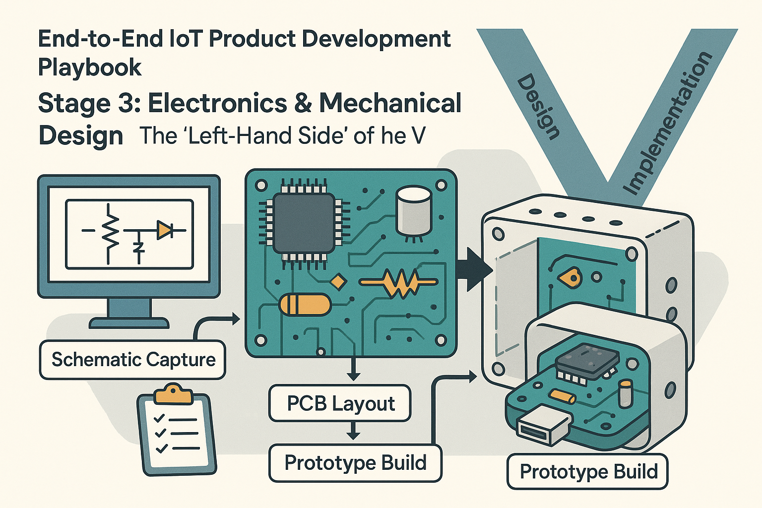
Now we’re getting to the hands-on fun: designing the actual hardware! Stage 3 is all about electronics and mechanical design, which often go hand-in-hand. If you’ve heard of the V-model in engineering (a classic development process model), the left side of the “V” is all about design and implementation – and that’s exactly where we are now. In other words, we’re focusing on designing the hardware that will later be verified and validated on the right side of the V. (Don’t worry if you’re not familiar with the V-model; the key idea is that hardware design tends to be a sequential process that you should approach with care. Once you print a circuit board or mold a plastic case, making changes is tricky – read: expensive 😬).
Stage 3 can be broken into a few sub-steps. Importantly, this is also the stage where hardware and software development start working in parallel (more on the software side in the next stage). On the hardware track, here’s how things typically unfold:
Schematic Capture: The Electronic Blueprint
Every electronic product begins as a drawing – not the artistic kind, but a schematic. Schematic capture is where the electrical circuit design is sketched out in detail using specialized CAD tools (such as Altium, Eagle, or KiCad). Think of the schematic as the blueprint for your circuit: it shows every component (microcontroller, sensors, capacitors, connectors, and more) and how they’re all electrically connected by nets (wires). It’s like mapping out a city of electronics where each component is a building and the nets are the roads connecting them.
This step is crucial because it’s much easier (and cheaper) to fix mistakes on a diagram than on a physical board. Once the schematic is drafted, a thorough review is a must. Typically, the engineer will export the schematic to a PDF and circulate it for peer review. Fresh eyes might catch something you missed – for example, “Oops, the temperature sensor’s power pin isn’t connected!” or “That resistor value looks off for the LED current-limiter.” Catching these issues now saves a lot of headache later.
At this stage some teams also perform an FMEA (Failure Modes and Effects Analysis) on critical parts of the design, like the power supply or safety circuits. FMEA is basically a fancy way of saying “Let’s imagine all the ways this circuit could fail and see what would happen.” For instance, what if the temperature sensor fails short-circuit (i.e., its two leads accidentally connect internally)? Would that just make the sensor read an extreme value, or could it damage the whole board by pulling too much current? By asking these scary “what-if” questions early, you can add protections or decide if the risk is acceptable. This kind of forward-thinking makes the device more reliable in the long run.
Meanwhile – and here’s where the parallel work comes in – the software/firmware team doesn’t have to wait idly for the hardware to be finished. Based on the schematic, firmware engineers can start creating a HAL (Hardware Abstraction Layer) or at least a skeleton of it. Essentially, they set up the software interfaces for the microcontroller’s peripherals (timers, communication interfaces like I2C or SPI for those sensors, etc.). They might even write unit tests or simulation code for these drivers on a PC. Imagine a developer writing code that fakes sensor readings just to test the logic – this way, the firmware team is already building the foundation. So, by the time the actual circuit board arrives, a lot of the code structure is ready and waiting to be tried on real hardware. This parallel effort means the software folks aren’t twiddling their thumbs; they’re laying groundwork that will make bringing up the hardware easier later.
PCB Layout: From Schematic to Physical Board
Once the schematic design is finalized and reviewed, it’s time to turn that electronic blueprint into a real-life circuit board. This is the PCB layout phase. Using another set of CAD tools (often the same suite used for schematics, like Altium or KiCad, which can switch to layout mode), the engineer places each component footprint onto a virtual board and starts routing the copper traces that connect everything. If the schematic is the blueprint, the PCB layout is the step where you decide exactly how that city of components will physically look – like deciding where each building sits and how the roads (wires) will run between them on the actual landscape of the board.
The outcome of PCB layout is a set of files (famously called Gerber files) that manufacturers use to fabricate the board. Another helpful output is a 3D model (often a STEP file) of the board. This 3D model is super useful for the mechanical design side of things – you can import it into your enclosure design to check that the board and all its components fit inside the product’s housing without any collisions (nobody wants a USB connector poking out where the case has no hole!).
During PCB layout, it’s critical to keep in mind Design for Manufacturing (DFM) and Design for Test (DFT) guidelines. In simple terms, DFM means designing the board so it can be manufactured reliably and cost-effectively, and DFT means designing it so it can be easily tested later on.
For example:
- DFM: Avoid placing components too close to the board’s edge or so tightly packed that assembly machines struggle to solder them. Ensure the layout can be manufactured without issues.
- DFT: Add test pads or a special connector so you can connect testing equipment or programmers to the board in production. This way, every unit off the line can be easily checked (imagine a convenient plug to program firmware or measure signals on each device).
It’s much easier to include these measures now than to realize later that you have a thousand finished units with no easy way to verify if they’re fully functional!
Many teams use a checklist during layout to ensure nothing is forgotten – things like adding fiducials (small marks that help automated assembly machines know how to align the board), maintaining proper clearances between high-voltage parts, labeling important connectors, and so on.
While the hardware team is busy routing traces and sweating the board details, the parallel software effort continues. The firmware team, knowing the exact sensor models and components from the schematic, can start writing actual driver code (or at least placeholders) against the datasheets of those components. They might use sensor emulators or write dummy code that mimics what the sensor would do. The cloud/backend team, if your IoT product has one, can also get ahead: for instance, setting up a basic cloud database and API endpoints to receive data from the device. Essentially, everyone is prepping their part of the puzzle so that when the first physical boards come in, it’s not a cold start for the rest of the team. By the time the PCB design is sent out for fabrication, your firmware might already have a “hello world” ready for the board and your cloud might have a little test server waiting to log the device’s first data point. This concurrent development really shortens the iteration loop later on.
Prototype Build: Bringing the Hardware to Life
With the PCB layout done and checked, it’s now time to go from digital files to physical objects. The first step is to get the boards fabricated. Typically, you send those Gerber files off to a PCB fab (there are many quick-turn PCB manufacturers who can produce boards in days). In parallel, you’ll want to make sure all the components that go on the board (the microcontroller, sensors, chips, etc.) are on hand. Pro tip: Order critical or long-lead-time parts as soon as you’re confident in your schematic and component selection! During global chip shortages, many teams learned this the hard way – you don’t want to be waiting 12 weeks for a particular sensor or radio chip while your boards are sitting there empty.
Once you have the bare PCBs and all the parts, you assemble a few prototype units. This could be done in-house if you have a well-equipped lab and a steady hand for soldering, or you might use an assembly service to solder all those tiny components on. The result is a set (often a small handful, like 1 to 5 boards) of prototype devices.
Now comes one of the most exciting (and nerve-wracking) moments in hardware development: bring-up, which is a fancy term for the first time you power on the board and see if it works. It’s common to do this carefully – for example, using a bench power supply with a current limit to avoid frying things if there’s a short circuit somewhere. Everyone in the lab might hold their breath as you flip the switch. Does the board power on without letting out the mystical blue smoke of burnt components? (Hopefully yes!)
After power-up, you methodically verify the basics. Are all the power rails at the expected voltages? (Check with a multimeter or oscilloscope.) Does the microcontroller (MCU) wake up and run code? A classic first test is often checking if a simple firmware that blinks an LED or sends a “Hello, world” message over a serial port is running. If you see that LED blink or get that message on your computer, it’s a huge victory – it means the heart of your board is alive and kicking.
Next, you’ll test communication with key peripherals: Can the MCU talk to the sensor over I2C or SPI as planned? Do the sensors return reasonable data? It’s at this stage you might discover issues. Maybe a sensor isn’t reading because of a wiring mistake or a subtle firmware bug. Bring-up is a detective game, where hardware and firmware engineers work together to troubleshoot any problems. For example, if the temperature reading is always zero, the firmware engineer might debug the code while the hardware engineer buzzes out the connections with a multimeter – together they’ll figure out if it’s a software initialization issue or maybe the sensor’s SDA and SCL lines got swapped on the PCB.
During prototype bring-up, you’re also watching out for any power or thermal issues. Is anything running hotter than it should? (Pro tip: carefully touching chips to feel for heat or using an infrared camera can catch hot spots.) Is the board drawing more current than expected (which could indicate something’s wired incorrectly or a component is faulty)? These tests ensure your prototype is not only working but also safe and performing within expected parameters.
If your device is meant to communicate wirelessly or meet certain regulatory standards (like FCC emissions for wireless gadgets in the US), this prototype stage is a good time to do some pre-compliance testing. This might mean taking the device to a lab to do a preliminary scan for radio frequency emissions to catch any big problems early. You don’t want to find out at the final certification test that your board is acting like an accidental radio transmitter at an unapproved frequency!
While the hardware team is busy with bring-up, the firmware team is now in full swing testing their code on the real device. All those drivers and HAL components they started earlier can be loaded onto the actual board. This is where the firmware might need some tuning – maybe the timing assumptions were a bit off, or an interrupt needs adjusting now that it’s on real silicon. If you’re using an RTOS (Real-Time Operating System) on the microcontroller, this is when you start tuning task priorities or timing, since on real hardware you can observe actual performance. The cloud team might also see the first real data coming through the system! For instance, the prototype might actually send a temperature reading up to a test server, confirming that the whole end-to-end flow (device -> cloud -> database) works at least on a small scale.
Stage 3 often involves a few iterations. It’s rare to get everything perfect on the first try – and that’s totally normal. You might find a mistake on the board (like a trace wired wrong or a component footprint error) that requires a little surgical fix on the prototypes (hello, bodge wires and patchwork fixes!), or it might be significant enough to warrant spinning a revised PCB for the next prototype round. Each iteration is a chance to improve: maybe you reposition a connector that was hard to reach, or you tweak the circuit to reduce noise on a sensor reading, etc. Don’t be discouraged by needing iterations; this is expected in hardware development.
Throughout this stage, close collaboration between hardware and software teams is vital. When an issue arises, both sides have to put on their detective hats and work together. Is the sensor not reading because the firmware’s wrong, or is there a solder bridge shorting something on the PCB? By communicating findings and hypotheses, the team can zero in on the problem faster. This collaborative troubleshooting is one of the most educational parts of the process – and it often strengthens the team’s understanding of the product as a whole.
Also, keep one eye on the future: if you plan to eventually manufacture this product at scale, use this prototype phase to think about manufacturing and testing for the long run. Remember DFM and DFT? Now’s the time to validate those decisions. For instance, if you included a programming header, try using it in a simulated production test: can you easily connect and program the board? If you added test pads, are they accessible to a bed-of-nails tester? It’s much easier to adjust your design for testability now than when you’ve got a production line running.
By the end of Stage 3, you should have one or more working prototype devices and a ton of lessons learned. You’ll have initial data on performance (like how much power does your device actually draw? Does the sensor perform accurately in real-world conditions?). You’ll likely also have a list of fixes or improvements for the next version. Most importantly, you’ve built the physical foundation of your IoT product – something you can hold in your hands and that actually works. 🎉
And hey, when that first prototype finally comes to life and sends data as expected, it’s perfectly fine to feel a bit like Dr. Frankenstein shouting “It’s alive!” in the lab. We all do a little happy dance at bring-up success. Just maybe don’t literally shout it too loud if you have lab neighbors or interns around – you don’t want to give anyone a heart attack! But definitely take a moment to celebrate – hardware is hard, and you’ve just cleared a huge milestone in your journey from idea to reality.