Author: TohumAB

  • End‑to‑End IoT Product Development Playbook -Stage 6: Verification & Validation – Did We Build the Right Thing (and Does It Actually Work)?

    End‑to‑End IoT Product Development Playbook -Stage 6: Verification & Validation – Did We Build the Right Thing (and Does It Actually Work)?

    Introduction to the V&V Phase

    Welcome to the final boss of IoT product development: Verification & Validation (V&V). This is where we answer two deceptively simple questions. Verification asks, “Did we build the thing right?”—does the product meet its specified requirements. Validation asks, “Did we build the right thing?”—does the product actually meet user needs in the real world. Treat them as complementary superpowers: one keeps you honest to the spec, the other keeps you honest to the customer

    Timing-wise, V&V kicks in post-integration and post–design freeze. By now, you’ve proven hardware and software can talk; you’re done adding features; and you’re ready to put the whole stack under a spotlight. Think of this phase as the final exam and graduation recital rolled into one: the device performs, the cloud sings harmony, and the app smiles photogenically. The goal is evidence—repeatable test results, traceable to requirements and user scenarios—that lets you ship with confidence rather than crossed fingers (IEEE, 2017; NASA, 2016).

    Layers of Testing: A Multi-Layered Gauntlet

    An IoT product is a stack: hardware (sensors, power, radio), firmware (embedded logic), and cloud/app (APIs, databases, dashboards). We verify each layer on its own merits, then validate the end-to-end system against user stories. Passing each layer is like beating a “mini-boss” on the way to the big fight.

    Hardware Verification: Torture Tests for Your Gadget

    Functional testing with fixtures (test jigs). First, prove the assembled device does what the schematic promised. A bed-of-nails fixture or pogo-pin jig makes fast work of exercising GPIOs, reading sensors with known stimuli, flashing firmware, and verifying power rails. Automate it so every board gets the same impartial interrogation. You’re building the same muscle you’ll need for end‑of‑line production tests later; your future manufacturing team will thank you (NASA, 2016).

    Stress and reliability testing (HALT). Next, the gym—and then some. HALT (Highly Accelerated Life Test) cranks temperature, vibration, and electrical stress well beyond normal operating conditions to flush out weak links before your customers do (Hobbs, 2008; Thermotron, n.d.; Accendo Reliability, n.d.). The point isn’t to “pass” so much as to discover: learn where the design cracks, fix the root cause, and build margin. If your device is rated 0–50 °C, you want to know how it behaves at −20 or +70 so the real world feels easy.

    Regulatory pre‑scans (EMC/ESD). Formal certifications (EMC emissions/immunity, ESD, radio, safety) can torpedo schedules if you discover problems at the lab. Do pre‑compliance checks now: measure radiated/conducted emissions in a basic setup, zap the device with ESD, and probe noisy lines. Early, iterative scans reduce risk and over‑engineering alike (Tektronix, n.d.; Interference Technology, 2017; Keysight, n.d.). If you hear an unexpected RF squeal, you can still add filters, tweak firmware duty cycles, or adjust PCB return paths—at prototype cost, not production cost.

    Benchmark vs. specs. Finally, check the deal you made with yourself. If you promised ±0.5 °C accuracy, prove it in a chamber against a calibrated reference. If you promised one‑year battery life, measure current in all modes and project realistically (including retries, OTA updates, and “oops, Wi‑Fi is flaky” scenarios). Verification at this level is the receipt for your Stage 1 requirements (NASA, 2016).

    Firmware Testing: Code Under a Microscope

    Unit tests. Firmware’s “atoms” are functions and modules; unit tests give them a conscience. Use a host‑based test runner or MCU‑aware framework to validate computations, state machines, and boundary conditions. Aim for high coverage—but remember: coverage finds untested code; it doesn’t prove tests are good. A policy like “~80%+ branch coverage” is pragmatic; chasing 100% often yields diminishing returns and brittle tests

    Integration tests on device. Put drivers, RTOS tasks, and comms stacks together and exercise them on real hardware. Feed a known voltage to an ADC and check the reported value; publish a synthetic payload and assert the device ACK flow; power‑cycle mid‑transfer and confirm correct recovery. Automate what you can so every firmware build faces the same impartial gauntlet (NASA, 2016).

    Static analysis and coding standards. Tools that read code without running it catch entire classes of bugs (buffer overflows, null dereferences, race hazards) and enforce rules (e.g., MISRA‑C subsets). In Stage 6, drive critical issues to zero and justify any waivers. This is cheap insurance for devices that must run unattended for months (IEEE, 2017).

    Fuzz and stress. Be an “evil user.” Fuzz inputs at the UART/USB/MQTT boundary, drop and restore networks repeatedly, overflow queues, and run for days to smoke out leaks and lockups. If you ship OTA, simulate bad connectivity, low battery, and mid‑update resets; make sure rollback works. The aim is not to show off—it’s to force rare states and prove the firmware fails safely and recovers predictably

    Cloud/API and UX Testing: The Other Half of the Puzzle

    Automated API tests. Every public interface—REST, MQTT topics, WebSocket endpoints—deserves executable tests for happy paths and weird edges (invalid payloads, expired tokens, missing fields). Bake them into CI; if an endpoint contract drifts, you’ll find out before customers do

    Security testing (OWASP). Apply OWASP Top 10 thinking to your web app and OWASP API Security Top 10 (2023) to your device and app APIs: broken access control, auth flaws, insecure design, and misconfiguration are perennial villains. Scan, pentest, and fix systematically; treat critical vulns as launch‑blockers

    Load testing and scale rehearsal. If you expect 1,000 devices at peak, simulate 2,000; test burst connects after an outage; vary message sizes, QoS, and TLS ciphers. MQTT brokers and back ends often behave differently at scale; better to discover queue starvation and hot partitions now.

    UX testing. Hand the mobile/web UI to fresh eyes. Can a first‑time user onboard a device without tribal knowledge? Are graphs accurate and units consistent? Does the alert say what happened, where, and what to do next? Validation doesn’t care that the database is normalized; it cares that the user smiles and succeeds.

    System Validation: End-to-End Boss Battle

    This is where we stop testing pieces and start testing stories: the thermostat that keeps the workshop warm, the cold‑chain sensor that texts when a fridge warms up, the leak detector that summons a plumber (well, sends an alert). Validation asks: Does the solution, as a whole, fulfill the job it was hired to do?

    End‑to‑end scenario runs. Take each user story from Stage 1 and run it for real. “As a facilities manager, I receive an alert within 60 seconds if freezer temp > −10 °C, and I can see a 24‑hour graph.” Drive the device hot, verify cloud ingestion, confirm alert delivery, and watch the UI. Repeat across networks, time zones, and device states.

    Requirements Traceability Matrix (RTM). Now, bring receipts. An RTM maps every “shall” to one or more verification artifacts (test case, analysis, inspection) so nothing is forgotten and nothing extra sneaks in. Here’s a plain‑text sketch:

    • R1: “Device shall connect to Wi‑Fi within 30 s.” → Test TC‑10 “Wi‑Fi timing” → Pass
    • R2: “System shall store hourly sensor readings for 12 months.” → Tests TC‑21 (retention), TC‑22 (query) → Pass
    • R3: “App shall display current sensor value within ±1 °C of reference.” → Tests TC‑30 (chamber), TC‑31 (UI format) → Fail (UI rounding bug; fix tracked)

    The RTM gives you a one‑glance coverage map from requirement to proof, which auditors, safety assessors, and your future self will love

    Beta trials (field validation). Lab success is necessary but not sufficient. Put devices in real environments with real users for a few weeks. You’ll learn things your lab can’t replicate: odd Wi‑Fi setups, creative human behaviors, environments at −15 °C, or the startling brightness of an LED in a dark bedroom. Close‑beta or open‑beta, collect structured feedback and crash/telemetry logs. Prioritize findings that block setup, data trust, or core value

    Pass/fail criteria and severity. Decide up front how you’ll exit Stage 6. A common bar is 0 open Severity‑1 issues, all requirements verified, and performance targets met. Severity frameworks such as IEEE 1044‑2009 help you keep bug impact discussions objective: Sev‑1 = showstopper/unsafe/unusable; Sev‑2 = major function impaired; Sev‑3 = minor/has workaround; Sev‑4 = cosmetic (IEEE, 2009). Use this to drive triage and go/no‑go with a clear head.

    Practical Advice and Final Thoughts

    Celebrate the passes; learn from the fails. A HALT‑hardened board, a firmware fuzz that runs for 72 hours crash‑free, an API test suite all green—those are mini‑victories. For failures, be grateful you found them here; the cheapest bug is the one you fix before customers meet it.

    Keep the user in the loop. It’s easy to “win the lab” but lose the living room. Beta feedback about setup confusion, noisy alerts, or mismatched units often yields small changes with huge perceived quality wins

    Treat V&V as an investment. Pre‑compliance and load rehearsals feel like extra work—until they save a month in certification or keep your launch day from sagging under a surprise device storm

    Document like a pro. Archive test plans, results, and RTM evidence. When you return for Stage 7 (compliance and manufacturing transfer), or v2.0 next year, you’ll be glad you left a breadcrumb trail.

    Coverage is a flashlight, not a trophy. Use coverage to find dark corners; don’t frame it as a single metric of quality. Balanced portfolios—unit, integration, end‑to‑end, and property‑based/fuzz—beat any one number

    When you can confidently say “Yes, we built the thing right” and “Yes, we built the right thing,” you’ve cleared the final gate. Onward to certification and launch—with fewer surprises, stronger evidence, and a product the team is proud to ship.


  • End‑to‑End IoT Product Development Playbook -Stage 5: Integration Gates – Making Sure It All Plays Nice Together

    End‑to‑End IoT Product Development Playbook -Stage 5: Integration Gates – Making Sure It All Plays Nice Together

    Picture an engineer hunched over a circuit board in a lab, carefully checking if the device comes to life. Integration Gates are those suspenseful moments in IoT development when all the pieces are finally combined and tested together.

    By the time you reach Stage 5: Integration, you’ve built hardware prototypes (from Stage 3) and developed iterative software/firmware builds (from Stage 4). Now it’s showtime – hardware, firmware, cloud services, and user applications all meet each other. Integration Gates are the key milestones in this stage – think of them like “checkpoint bosses” in a video game. You don’t advance to the next level until you’ve proven certain capabilities at each gate. These gates turn what could be a scary big-bang system integration into a step-by-step confidence builder. It’s a mix of excitement and anxiety as you power everything on and watch for sparks (hopefully only metaphorical ones!). The idea is to catch problems early and incrementally, rather than discovering a pile of issues right before launch. Given that IoT products involve multiple components developed somewhat independently – hardware, firmware, cloud, mobile apps – unexpected compatibility issues often pop up when everything is integrated. Integration Gates help prevent “half-baked” subsystems from cluttering up the final system by enforcing that each piece meets certain criteria before moving on.

    Let’s walk through the typical integration gates in an IoT project, and see why each is important. At each gate, we’ll verify that different parts of the system “play nice” together:

    Bring-Up Gate – Getting the Basics Working

    The first sign of life – a simple dev board with an LED blinking is often the Hello World of hardware integration.

    The Bring-Up Gate is the first (and very basic) integration test with the real hardware. The goal at this gate is humble and fundamental: Does the microcontroller (MCU) on our board boot up and run code? This is akin to checking the patient’s pulse 🩺 – is the device alive at all? Here’s what happens at this gate:

    • Flashing Firmware & Booting: You attempt to flash the initial firmware onto the device and then reset it. Does it start executing code? A common practice is to load a firmware that makes an LED blink or sends a simple "Hello, world" message over a serial console. If you see that little LED blinking on your board, you know the heart is beating. It confirms that the core hardware (power supply, clock, MCU) is operational and that your programming toolchain can successfully load code into the device’s memory.
    • Basic Hardware Functionality: Next, you check that the device can perform a few rudimentary tasks on its own. For example, can it read a basic sensor on the board or at least measure something like its own battery level or supply voltage? Can it communicate over a debug interface (such as printing to a serial console or logger)? At this point, you’re ensuring that fundamental I/O and peripherals are working – e.g. GPIO pins can toggle (hence the LED blink test), the CPU isn’t crashing, and maybe the buttons or basic sensors respond.

    Essentially, the Bring-Up Gate is confirming the board is not a “brick.” Passing this gate means the patient is alive and responsive: the hardware is powered properly, the MCU runs code, and you have a working line of communication for further testing. This might sound trivial, but it’s a huge relief the first time it happens. Often, engineers hold their breath when powering on a custom board for the first time – if something is wrong (say, a miswired power rail or an incorrectly soldered chip), the board might do nothing or show erratic behavior. By blinking an LED or printing a message, you’re victoriously yelling, “It lives!”

    Why it matters: Bring-up is the safety net that catches fundamental issues early. If the board doesn’t boot or the firmware can’t run, that’s a show-stopper which you need to fix now. Maybe the power circuitry is faulty, or the oscillator for the clock isn’t oscillating – better to find out immediately. Only after you pass this gate do you proceed to more complex integration. In project terms, this gate verifies some of the most basic requirements (remember those Stage 1 specs about hardware power and processing?). It ensures your hardware design and basic firmware can support the next steps. After a successful Bring-Up Gate, you can confidently say, “Alright, the lights are on and someone’s home. Onward to sending some real data!”

    Data-Path Gate – From Device to Cloud (The Core Journey)

    After confirming the device is alive, it’s time to test the core reason the whole IoT system exists: getting sensor data from the device all the way to the cloud. The Data-Path Gate focuses on the end-to-end data pipeline. This is where you prove that your IoT device can actually fulfill its primary mission of collecting data and transmitting it to a backend service.

    Imagine our device is a temperature sensor. At the Data-Path Gate, you would do something like this: trigger the sensor to take a reading (perhaps by heating the sensor slightly or simulating a change in temperature), and then watch the system to see that this reading travels from the sensor -> device -> network -> cloud -> database. It’s a full vertical slice of functionality. You want to verify a number of things along this path:

    • Sensor Integration: The firmware is able to read data from the sensor correctly. For instance, if the sensor says the room is 25°C, the device’s software should obtain that value (and maybe timestamp it).
    • Network Transmission: The device successfully sends the data over its communication interface. Whether it’s Bluetooth Low Energy, Wi-Fi, cellular, LoRaWAN, or another wireless link, that radio or network module needs to work now. At this gate, you test that the device can connect to the network (pair with a gateway or join Wi-Fi, connect to cellular, etc.) and actually transmit the sensor data outward. You might send the data as a packet via MQTT, HTTP, or whatever protocol your IoT system uses.
    • Cloud Reception and Storage: On the other end of that transmission, your cloud backend (server, IoT platform, etc.) should receive the data and deposit it in the right place – for example, in a cloud database, data lake, or time-series storage. Here you’ll check that the data arrives intact and is stored or queued as expected. If the temperature was 25°C, does the cloud record show 25°C (and not some gibberish)? Are the timestamps correct?

    A typical IoT data path: devices gather sensor readings, communicate over the internet, and update cloud services or databases, which in turn feed user applications. The Data-Path Gate proves this whole pipeline works in your product.

    Passing the Data-Path Gate usually means the end-to-end data pipeline works in practice, not just in theory. It’s a major milestone because it demonstrates that your architecture is sound: the device’s hardware and firmware can talk to the cloud infrastructure. Essentially, you’ve shown that “Yes, our device actually talks to our cloud!” and that the fundamental value proposition – collecting data remotely – is achievable.

    During this phase, you also evaluate data quality and performance: Are the sensor readings making it to the cloud in a timely manner? For example, if your requirement was to send an update every 10 minutes, check that this interval is being met. Verify that the data isn’t corrupted or lost in transit. Perhaps you generate a known test pattern or range of sensor values and confirm the cloud receives the same pattern. If something is off (maybe the values look wrong due to a unit conversion bug, or messages take too long due to network issues), you catch it now. It’s much easier to tweak and fix these issues at this stage than to discover later that your device has been silently dropping data.

    Real-world example: Suppose you have a humidity sensor that should send data every 10 minutes. At the data-path test, you notice the cloud is receiving irregular updates – sometimes 10 minutes, sometimes 30 minutes apart. Investigating now might reveal a power-saving feature in the firmware that put the device to sleep longer than expected, or perhaps a connectivity dropout. You can then adjust the firmware or network settings before proceeding. Without a Data-Path Gate, such a problem might only be noticed during a full system test or pilot trial, which could be chaotic to debug.

    In terms of requirements, by the time you pass the Data-Path Gate, all those specifications related to data transmission and sensing (the ones defined back in Stage 1) should be verified as “met in testing.” You can check off requirements like “Device shall transmit temperature readings to cloud database within X minutes of sensing” as done. This gives everyone confidence that the backbone of the IoT system is solid.

    User-Story Gate – End-to-End User Experience Check

    Now we step fully into the user’s shoes. It’s not enough that data lives in a cloud database – the User-Story Gate asks: Can a real end user actually benefit from this data? In other words, does the whole system deliver a meaningful use case from the user’s perspective.

    At this gate, you integrate the front-end application (which could be a mobile app, web app, or other user interface) with the rest of the system. The idea is to demonstrate a real-world scenario or user story working seamlessly with your IoT device and cloud. For example, a common user story might be:

    “As a user, I open the mobile app and see the current temperature reading from my device, and I get an alert if the temperature exceeds 30°C.”

    To pass the User-Story Gate, you would actually do that:

    • Open the app or dashboard as an end user.
    • Confirm that you can view the live data coming from the device (which, thanks to passing the Data-Path Gate, is populating the cloud backend).
    • Perhaps manipulate something to trigger an alert or action: for instance, force the temperature high and see if the system sends a notification or highlights the reading in the app’s UI.

    In practice, this might involve building a simple UI screen that fetches data from your cloud database or via an API. If our product is an IoT home thermostat, the user-story test might involve seeing the current temperature on a smartphone app, along with a graph of the last 24 hours, and maybe toggling a setting to ensure the device can receive commands too (if applicable). The key is that the product becomes demo-able in a meaningful way. You could take your device and app to a non-engineer – say a project stakeholder or a friendly beta tester – and they would be able to use it in a basic but real scenario.

    Why it matters: This gate is often the first time everything (hardware, firmware, cloud, and user interface) is working together. It’s a true integration test of the full system including the human element. From a development perspective, it forces the team to connect all the dots:

    • The app needs to have the correct endpoints or database access to retrieve the data.
    • The cloud backend needs to expose the data in a form the app can use (for example, REST API or WebSocket).
    • You also check that data is not only present but makes sense to the user. Is the unit of measure clear? Is the data updated reasonably fast on the UI after the device sends it? If a user has to wait too long to see an update, that might be a problem to address (maybe the update frequency needs tuning or the app needs to poll more often or use push notifications).

    By passing the User-Story Gate, you demonstrate that your IoT product isn’t just a theoretical system—it actually delivers value to an end user. This is a huge morale booster for the team. It’s often the point where the project becomes real for people outside the dev team. You might gather around to show the company’s product manager, “Look, here’s your data on the app!” and that’s a moment of celebration.

    From a project management angle, at this gate you’ll verify requirements related to user experience. For example, if you had a requirement that “A user shall be able to view the device’s readings remotely via a mobile application”, well, now you can mark that as tested and met. You might also test basic user-level functionality like account login, device provisioning (did the user need to pair the device or add it to their account?), and any alerts or notifications. Essentially, you’re checking off the user-facing functionality items on your checklist.

    Additionally, this gate can reveal any last-mile issues: maybe the data format needs tweaking for the UI, or perhaps you discover that the average user can’t interpret a raw sensor reading and you decide to add some more info or adjust the UI. Those insights are invaluable and are much easier to handle now than if discovered after a product launch.

    Design-Freeze Gate – Locking Down the Final Design

    The Design-Freeze Gate is a slightly different beast than the previous integration gates. Up to now, each gate was about demonstrating new end-to-end capabilities. Design freeze, however, is about reaching a point of confidence and saying, “Alright, no more big changes – this is the design we’re going to finalize and push towards production.” In the context of an IoT project, this typically means both the hardware design and the firmware/software feature set are declared “frozen” (no further changes except critical fixes).

    By the time you’re approaching design freeze, you’ve likely gone through one or more iterations of your hardware. For example, you might have built an EVT (Engineering Validation Test) prototype and then a DVT (Design Validation Test) unit in earlier stages. Each iteration got you closer to the final form. A design freeze generally happens when you believe the current design is good enough to advance into the final manufacturing steps. This includes things like ordering the production PCBs, committing to the enclosure design and tooling, and finalizing the component selection. On the firmware side, design freeze means you have implemented all planned features – from here on out, you plan to do only bug fixes, optimizations, or cosmetic tweaks. No new features that would alter the system’s behavior in a major way.

    Why freeze the design? Because after this point, changes become very expensive or time-consuming. Imagine you freeze and then send your PCB design out for a mass production run of 10,000 units, and then you realize you forgot a critical sensor or wired something incorrectly – that’s a nightmare scenario. The goal is to avoid that by thoroughly vetting the design before freezing. Once you freeze, any modification might mean spinning a new circuit board (with all the cost and delay that entails) or updating a mold for the enclosure, or redoing certifications. One manufacturing guide notes that by the final pre-production stage (often called PVT – Production Validation Test), the product design is indeed “frozen” because it’s already been validated by prior testing (EVT/DVT) and changes at that point could disrupt the production linetitoma.com. In other words, you freeze when you are confident that the design meets requirements and can be produced at scale without issues.

    Before declaring design freeze, teams often perform a comprehensive review. This might involve revisiting the original requirements and verifying that every single requirement has been addressed and tested at least once. Any outstanding issues should be very minor or have acceptable workarounds. For example, maybe during DVT you discovered a minor issue like an LED being a bit dim – but it doesn’t affect functionality, and you decide that’s acceptable. Or perhaps a certain sensor’s reading was slightly noisy, and you addressed it in firmware by averaging readings. The design freeze review will catalog all these findings and solutions. It’s also common to run final performance tests and reliability tests at this stage (like battery life measurements, environmental tests, etc.) to be sure nothing was overlooked.

    A part of design freeze is also ensuring you meet all regulatory and certification requirements. By now, you should have either completed or be ready to complete tests for things like EMC (electromagnetic compatibility), safety (e.g. UL certification), radio certifications (FCC, CE, etc.), and any industry-specific standards. The hardware design should include any tweaks needed to pass these (for instance, added shielding or filter components to reduce noise, which you would have verified in DVT). Once you freeze, you’ll send hardware off for official certification if you haven’t already – doing that after freeze is logical because you don’t plan to change the design that could alter compliance.

    Passing the Design-Freeze Gate is a significant milestone. It signals that the team believes the current product design meets the requirements well enough to proceed to manufacturing and launch. After this gate, the project typically moves into a new phase: building pilot production units, final verification testing on those units (often called PVT as mentioned), and ramping up manufacturing. The mindset shifts from development to production and deployment.

    In summary, at Design-Freeze Gate, you lock in the following:

    • Hardware is final: No further changes to schematics or PCB layout. You’re ready to order the “real” manufacturing run with this design. (If a problem is found later, it might result in a Version 2.0 down the road or a patch, but not now).
    • Firmware is feature-complete: All planned features are implemented. Any new ideas go to a future roadmap; for now, you focus on fixing bugs and polishing what’s there. You might branch the code in version control, labeling this as a release candidate.
    • Documentation is updated: You’ll freeze things like the BOM (bill of materials), production test plans, user manuals drafts, etc., reflecting the final design.
    • No loose ends in requirements: The requirement checklist from Stage 1 should be essentially all green. Maybe a few low-priority enhancements are deferred, but anything critical is done or you consciously sign off that it won’t be done.

    Design freeze can feel a bit nerve-wracking – you’re essentially betting that you’re satisfied enough with the product to go out to the world. But it’s also exciting; it means you’re entering the home stretch of the project.

    Managing Integration Gates and Reviews (Staying on Track)

    How do teams actually manage these gates? Typically, milestone review meetings are held at each gate. The format is often formal: you gather the key stakeholders (product managers, engineers, QA, etc.) and review a checklist of criteria that must be met for the gate. Remember those Stage 1 requirements and the acceptance tests or verification methods you defined for each? This is where they become really useful. For each integration gate, you map which requirements or goals should now be fulfilled and verified.

    For example:

    • Before Bring-Up Gate: Requirements about basic hardware functionality (e.g., “MCU shall boot and execute firmware”, “Device shall provide a hardware interface for debugging”) should be tested and checked off.
    • By Data-Path Gate: All requirements related to sensor data capture and transmission (e.g., “Device shall measure temperature within ±1°C accuracy”, “Device shall transmit data via Wi-Fi to cloud within 1 minute”) must show as met. You would demonstrate tests for each of those during the review.
    • By User-Story Gate: Requirements related to user interactions (e.g., “User shall be able to view current and 24h history of data via the app”, “System shall alert user when data goes out of range”) should be completed and demonstrated.
    • By Design-Freeze Gate: Essentially all remaining requirements should be either met or formally agreed to be out-of-scope. This includes hardware durability, regulatory compliance, battery life, etc. Also, any open bugs of severity High/Critical should be resolved or have a plan, since after this you don’t want surprises.

    During the gate review, each item on the checklist is discussed. If it’s met, great – you provide evidence (test results, demo, etc.). If something is not met, the team has to decide: is this a deal-breaker for moving forward? In a disciplined process, you do not simply wave it off with “Oh, we’ll fix that later, let’s move on.” Instead, you log it as an action item and address it before fully considering the gate passed. Maybe it means delaying the schedule slightly to fix the issue or come up with a workaround. This discipline prevents a pile-up of unresolved problems at the very end. It’s so tempting to say “That part’s not working yet, but it’s minor, we’ll handle it eventually.” The integration gate approach urges you to resist that temptation! Each gate is like a safety net catching problems when they’re easier (and cheaper) to fix – i.e., now, not when you’re in a panic right before launch.

    Teams often use project tracking tools or simply spreadsheets for these checklists. For instance, you might have a spreadsheet with all requirements as rows, and columns indicating status at Bring-Up test, Data-Path test, etc. It provides a clear snapshot of where you stand at each milestone. Some organizations also assign a “gatekeeper” role – a person (or committee) who must sign off that the criteria are met. This ensures accountability. It’s not meant to be bureaucracy for its own sake, but rather a way to maintain quality and avoid rushing ahead with latent flaws.

    Another practice at integration gates is to reflect on lessons learned so far. Maybe at the Data-Path Gate review, the team discusses “What problems did we hit getting data to the cloud, and how can we prevent similar issues going forward?” These discussions might lead to adjustments in the development process or test coverage for the next stages. For example, if you found a lot of problems with network connectivity, you might beef up that part of your test plan for future units or add additional monitoring.

    Step-by-Step Integration vs. Big-Bang: Why Gates Matter (Wrap-Up)

    Integration Gates might seem like extra checkpoints that slow things down, but in reality they de-risk your project in a big way. Without gates, you might be tempted to build each part of the system in isolation and only try everything together at the very end – that’s the classic big-bang integration. In complex IoT projects, big-bang integration is a recipe for sleepless nights and nasty surprises. By contrast, the gated approach breaks the problem into manageable chunks. At each gate, you’re effectively saying “We’re not proceeding to the next phase until we’re confident in the current one.” This approach has proven valuable in both hardware and software industries to catch issues early.

    Think of it like climbing a mountain via base camps. Each Integration Gate is a base camp where you check your equipment and health before ascending higher. You wouldn’t attempt the summit if you realized you forgot your oxygen mask at base camp 2 – similarly, you don’t want to attempt full production if you haven’t verified your device can talk to the cloud since Stage 5!

    By the time you hit the Design-Freeze Gate, you should feel a sense of accomplishment: you’ve systematically ironed out the major kinks. The device boots reliably, it communicates properly, users can use it and find value, and the design is solidified. Of course, the journey isn’t over – after design freeze comes stages like certification testing, pilot production runs, and eventually mass production and deployment. But thanks to the integration gates, you enter those final stages with much higher confidence. You’ve essentially built up the system’s reliability step by step, instead of throwing everything together blindly.

    It’s also worth noting the positive psychological impact on the team. Each gate passed is a mini-celebration opportunity 🎉. In a long hardware project, morale can dip during the grind, so these milestones give a chance to acknowledge progress. When the first board boots up (Bring-Up Gate) – that’s often donuts or high-fives all around. When data shows up in the cloud (Data-Path Gate) – maybe a team lunch to celebrate. When the first end-to-end demo works (User-Story Gate) – that’s a huge validation of everyone’s efforts. By the final design freeze, you might finally allow yourself a toast (though perhaps hold off on the expensive champagne until everything is truly in mass production!). These small wins keep everyone motivated and aligned.

    In conclusion, Stage 5: Integration Gates ensure that all the components of your IoT product “play nice” together before you move forward. They enforce a structured way to validate functionality incrementally, catch and resolve issues early, and align the team on meeting the product requirements. It transforms a potentially daunting integration process into a series of achievable steps. So when you embark on developing an IoT product, remember to tackle those checkpoint bosses one by one – you’ll save yourself a lot of headaches and have more reasons to celebrate along the way. Now, onward to the next stage (and eventually, to product launch glory)! Each gate conquered brings you one level closer to a successful IoT product. Level up! 🚀

    Sources: The importance of phased validation in IoT developmenttitoma.com, and typical IoT system architecture involving devices, communications, cloud, and user apps. Integration challenges often arise when separately developed components come together – a problem mitigated by using integration gates to gatekeep progress.

  • End‑to‑End IoT Product Development Playbook -Stage 4: Firmware & Cloud Software Development

    End‑to‑End IoT Product Development Playbook -Stage 4: Firmware & Cloud Software Development

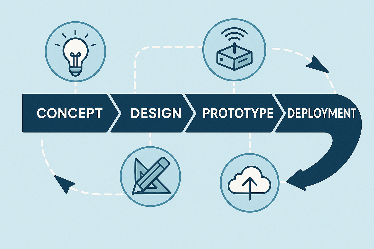
    Welcome to the right-hand side of the V! In the classic V-model of product development, the left side is about design (which we tackled in previous stages) and the right side is about implementation and testing. In Stage 4, we dive into developing the firmware (the software running on your IoT device) and the cloud software (servers, databases, APIs, user interfaces) that together bring your product to life. Unlike hardware development, which is relatively inflexible once printed on a circuit board, software development is highly iterative and agile. In fact, you may have already written bits of firmware back in Stage 3 while testing your hardware design. Now it’s time to ramp that up. The beauty of software is that it’s like clay – easy to mold and change on the fly – so we can iterate quickly and refine continuously. This stage will run in parallel with any remaining hardware work, each informing the other as needed.

    Stage 4 can be thought of in two main parts: first planning the software architecture and design (to set a strong foundation), and then an ongoing cycle of development sprints where we build, test, and repeat until the software is solid. Let’s break it down.

    4.1 Software Architecture & Design

    Before everyone jumps into coding like there’s no tomorrow, it’s wise to sketch out a game plan for the software architecture – for both the firmware on the device and the cloud components. Think of this like planning a road trip. You wouldn’t just start driving without a map; similarly, we sketch out the major components and how they interact before we write thousands of lines of code. This is analogous to the system architecture we did in Stage 2, but now at the code level. Good software architecture planning will save you from the dreaded “spaghetti code” monster later on. Here are the key things to establish in this phase:

    Firmware Architecture (Layered Approach and RTOS Considerations)

    Define the structure of your embedded code by layering it. A common approach in firmware is a layered architecture, which helps organize code logically and makes it easier to maintain. For example, at the lowest level you might have a Board Support Package (BSP) or hardware abstraction layer – this contains low-level drivers specific to your microcontroller and hardware peripherals. Above that, you might have device drivers or modules for your sensors and actuators (handling things like reading a temperature sensor or driving an LED). Above the drivers, you could have a services layer – this might implement communication protocols, data processing algorithms, or other logic that processes the raw data. Finally, at the top, you have the application layer, which is the brains of your device: it ties everything together to fulfill your product’s purpose (e.g. reading sensor values, making decisions, sending data to the cloud, and reacting to commands). Consider drawing a simple diagram (UML component diagram or even just boxes and arrows on a whiteboard) to visualize these layers. This helps everyone on the team understand the separation of concerns – like building a house with a foundation, framing, and roof, each layer has its job.

    Another big architectural decision on the firmware side is whether to use an RTOS (Real-Time Operating System) or not. An RTOS is like having a small operating system on your device that can run multiple tasks seemingly at the same time (via scheduling). If your device only does one thing at a time, you might not need an RTOS. But most IoT gadgets have a lot going on concurrently – for example, reading sensors periodically, listening for incoming messages (from cloud or user input), updating a display or LED, and handling network communication. With an RTOS, you can design your firmware as a set of tasks or threads. For instance, you could have one task dedicated to sensor sampling, another dedicated to handling communications (sending data or receiving commands), and another for housekeeping or user interface updates. As part of your architecture design, outline these tasks and how they will communicate with each other – common mechanisms include message queues, event flags, or shared data protected by mutexes (to avoid conflicts). Deciding this early will help ensure your firmware doesn’t become a tangle of interwoven code where everything depends on everything else (a.k.a. spaghetti code). Instead, you’ll have clear interfaces: maybe the sensor task puts new readings into a queue, and the communication task picks them up to send to the cloud. If you design these interfaces clearly now, coding will be much smoother and you’ll thank yourself later when it’s time to troubleshoot or extend the firmware.

    Why all this architectural fuss for firmware? Because it makes your life easier down the road. With a good layered design and task structure, you can modify one part (say, swap out a sensor driver or tweak an algorithm) without breaking everything else. It also makes it easier for multiple developers to work together without stepping on each others’ toes – one person can develop the sensor driver while another works on the cloud communication code, as long as you’ve agreed how those parts interface (e.g. the data format of a sensor reading message). In short, a little planning here helps avoid a lot of pain later.

    Cloud Architecture (Server, Database, and Application Structure)

    Now let’s consider the cloud side. The IoT device doesn’t live in isolation – it’s usually talking to some cloud service or server. Similar architectural thinking is needed here: sketch out the major components of your cloud software. For example, you might have an API server that receives data from devices and also serves requests from user applications. There will likely be a database where you store device data (sensor readings, device statuses, user info, etc.). There may be additional services or microservices doing data processing or analytics – for instance, analyzing the data for anomalies, triggering alerts or actions when certain conditions are met (e.g. send an email if a temperature reading is too high), or performing aggregations for reporting. On top of this, consider the client applications: perhaps a web dashboard or a mobile app that users interact with. Those clients will communicate with the server (often via the API) to display data and send user commands (like a user pressing a button to turn on their IoT light bulb from their phone).

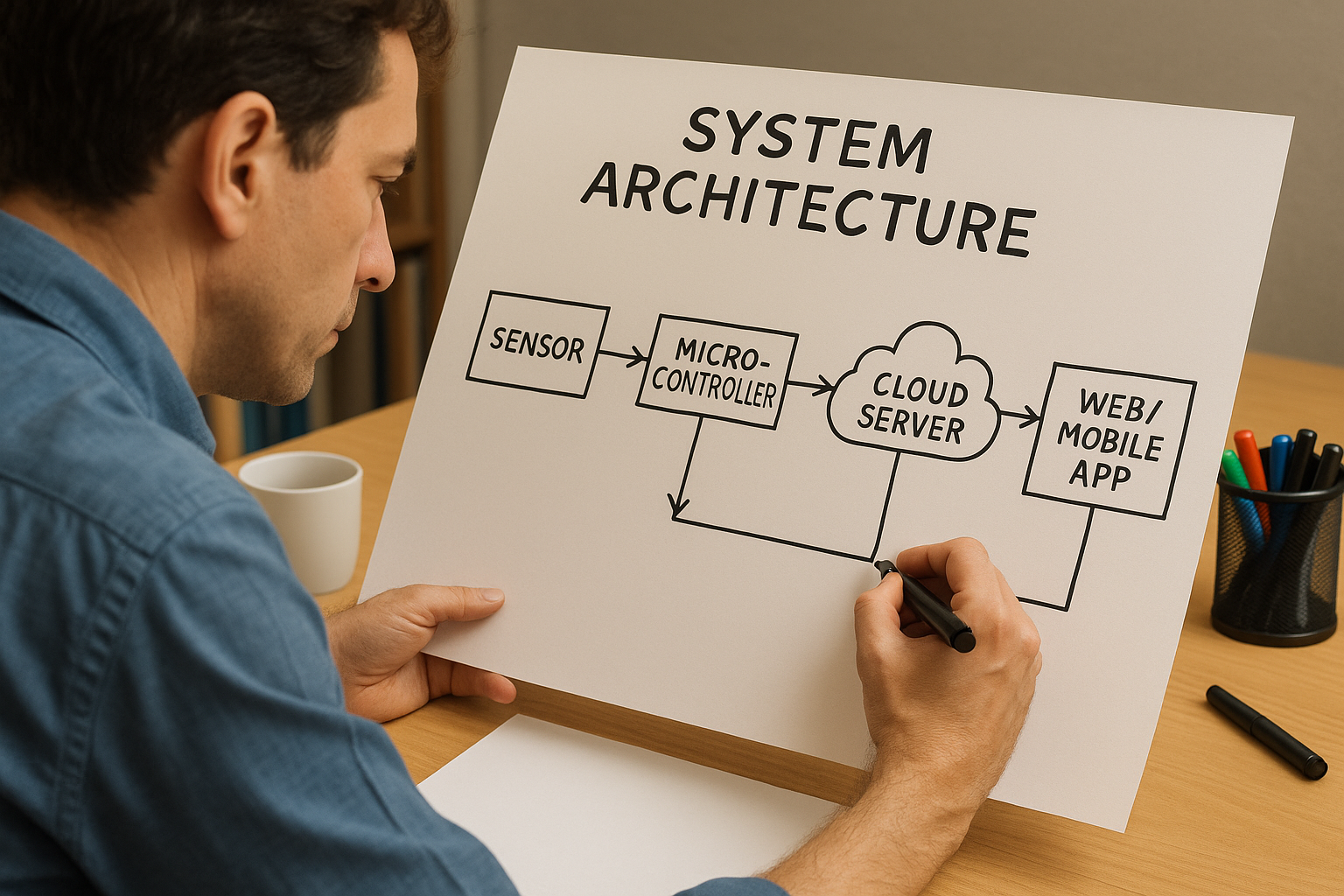
    It’s helpful to draw a diagram of this ecosystem – the C4 model (Client-Container-Component-Code) is a popular way to diagram software architecture. At least draw the Container level: show the device, the server, the database, and the client app, and how data flows between them. For example, your diagram might have an arrow from Device to Cloud API (“sends sensor data via HTTP/MQTT”), an arrow from Cloud to Database (“stores data”), and an arrow from Client App to Cloud (“user requests data or sends command”), and so on. This visual map ensures everyone (firmware developers, cloud engineers, frontend developers, etc.) has a clear mental model of how things connect. It’s much easier to discuss and catch design issues early with such a diagram in hand. Perhaps you discover in this stage that you need an additional component – for instance, a message broker or IoT platform service – to handle scaling to many devices. Better to think of it now than when you’re deep in coding.

    One more aspect: think about scalability and reliability in your cloud design. If you expect 100,000 devices connecting eventually, can your chosen database and server design handle it? If a server goes down, what happens (do you have redundancy)? Those details might be fleshed out more in a later stage, but the high-level design should account for major concerns like that up front. For example, you might decide to use a cloud IoT platform (AWS IoT, Azure IoT Hub, etc.) instead of building everything from scratch, which would become part of your architecture decision.

    Communication Protocols & Data Formats (Device-Cloud Communication)

    An IoT product inherently involves communication between the device and the cloud. Part of the software design is deciding how they talk to each other and in what language (protocols and data formats). There are a few common protocol choices in IoT: for example, will your device use MQTT, HTTP/REST, CoAP, or maybe something like WebSockets? Each has its pros and cons. MQTT is a lightweight publish/subscribe protocol great for IoT because it’s efficient and works well over unreliable networks – many IoT systems use it for device-to-cloud messaging. HTTP/REST is very common and easy to test (since you can hit it with standard web tools) but might have a bit more overhead per message. CoAP is a specialized IoT protocol similar to a lightweight HTTP, often used in constrained networks. The key is to choose one that fits your device’s capabilities and your cloud infrastructure. For example, if you have a super constrained device (8-bit microcontroller on battery), maybe MQTT or CoAP is better than HTTP. If your device is pretty capable (like running Linux or similar), HTTP/REST could be fine and more straightforward.

    Once the protocol is chosen, design the data format for messages. Many projects use JSON because it’s human-readable and easy to work with (most languages have JSON parsers). For instance, a temperature reading message in JSON might look like:

    { "device_id": "ABC123", "timestamp": 1692124800, "temperature_c": 22.5 }
    

    This clearly lays out fields. JSON is a tad verbose though, so if your device needs to send data super efficiently (think thousands of messages or very low bandwidth), you might use a binary format (like Protocol Buffers, CBOR, or a custom binary scheme) to save bytes. The design choice here will affect both firmware and cloud: both sides must agree on the protocol and format. It’s a bit like agreeing on a language before starting a conversation – if the device “speaks” MQTT+JSON and the server expects something else, they won’t understand each other.

    A helpful tool at this stage is to draw a sequence diagram or just write out an example sequence of communication. For example: “Device takes a sensor reading, formats a JSON payload, sends it via MQTT to topic X; Cloud broker receives it, the cloud service processes and acknowledges it, then stores it in the database; later, a user requests data via the app, the cloud API fetches from the database and returns JSON to the app.” Writing this flow out ensures everyone (the firmware dev and cloud dev, especially) are literally on the same page about how the data moves around. It can prevent miscommunications like “Oh, I thought we were using UNIX timestamp in seconds, not milliseconds” or “Were we compressing the data or not?”. Catch those now in design, it’ll save debugging time later.

    Coding Standards and Team Tools (Quality from the Start)

    Now, let’s talk about how we will write code and collaborate, because having the whole team follow common practices is super important. Agree on coding standards for each part of the system. For embedded C development, many teams adopt MISRA-C guidelines – that’s a set of rules for the C language aimed at avoiding unsafe or bug-prone constructs (originally from the automotive industry, but widely useful in any critical firmware). If you’re using C++ in firmware, you might decide which features of modern C++ are allowed or banned (to keep things safe for embedded systems – for example, maybe avoiding dynamic allocation at runtime, etc.). For higher-level languages on the cloud side like Python, you’d probably follow PEP 8 style guide, and for JavaScript/TypeScript maybe use a linter with the Airbnb style or whatever is standard. The goal isn’t to be nitpicky, it’s to ensure consistency and catch common pitfalls. When everyone writes in a consistent style, the codebase feels like one product rather than a patchwork, and it’s easier to read and maintain code written by someone else on the team.

    In addition to coding style, choose the tools and infrastructure the team will use. This includes version control and repository setup (almost certainly Git – if you’re not already using it, definitely do, as it’s the backbone of collaborative coding). Decide on the branching strategy: will you use a simple trunk-based development, or GitFlow with feature branches, etc.? Also, set up an issue tracking system if you haven’t (like Jira, Trello, Asana, or GitHub Issues) to manage the tasks and user stories in your sprints. It’s also a good time to set up the Continuous Integration (CI) pipeline: choose a CI service (GitHub Actions, GitLab CI, Jenkins, CircleCI, etc.) and configure it to automatically build and test your code whenever changes are pushed. We’ll talk more about CI in the next section, but the architecture stage is where you make sure all developers have access to these tools and know how to use them.

    Another part of “code culture” is deciding on things like code review practices – e.g., will every pull request require at least one other developer to approve it? Setting these expectations early is healthy. It might feel formal, but it saves you from scenarios where someone’s unreviewed code introduces a nasty bug or security hole that others only catch much later. By agreeing that “we always do code reviews, follow the style guide, and run the tests before merging”, you instill a quality mindset from day one. Modern development is as much about team collaboration and discipline as it is about coding genius.

    Finally, remember that this Stage 4.1 planning is not about drawing pretty diagrams no one ever looks at – it’s about giving the team a shared understanding and a technical roadmap. It’s like planning a road trip route and packing a map: you know where the big turns are and how you’ll navigate, but you can still be flexible with pit stops or detours. Spend a reasonable amount of time on this architecture design, but don’t aim for perfection or detail every last function. You want just enough design that people can start coding in a coordinated way. With this foundation laid, you’re ready to jump into development with confidence.

    4.2 Development Sprints – Iterate and Conquer

    With the architecture blueprint in hand, now the fun begins – writing code, testing it, and seeing your IoT product actually do stuff! We approach this in iterations, typically using sprints as in Agile methodology. A sprint is a short, fixed-length cycle (commonly 2 weeks, but it could be 1 week or up to 4 weeks depending on your team’s preference) where the team commits to delivering a set of features or improvements by the end. The idea is to break down the massive job of “develop all the software” into bite-sized chunks that we can steadily tackle and make tangible progress on.

    This iterative approach has huge benefits: it forces continuous integration of components (so firmware and cloud software are tested together frequently), and it gives you many opportunities to get feedback and adjust course if needed. It’s much better than coding for 6 months and only then trying to see if it all works (which is a recipe for unpleasant surprises). Let’s see how a typical sprint cycle might look for our IoT product development:

    Sprint Planning & User Stories

    Each sprint starts with a Sprint Planning meeting. The team looks at the product backlog – this is the master list of all features, fixes, and tasks to be done, which was initially derived from the requirements we gathered back in Stage 1 (and added to as we learned more in later stages). In planning, the team selects a set of user stories or tasks from the backlog to tackle in the sprint, based on priority and the team’s capacity.

    A user story is a bite-sized description of a feature from an end-user’s perspective, often following the template “As a <user type>, I want <some ability> so that <benefit>.” For example, one story might be: “As a user, I want the IoT device to send temperature data to the cloud every 10 minutes, so I can monitor my room’s temperature remotely.” From this story, the team will figure out what needs to be done on both the device and cloud side: perhaps on the device firmware, we need to read the temperature sensor and send an MQTT message every 600 seconds; on the cloud, we need an API or message handler to receive that data and a place to store it, and maybe a simple interface to display it.

    During sprint planning, the team discusses each chosen story to nail down the acceptance criteria – basically, how do we know when this story is “done” and working? For the above example, criteria might be: “Given a device with a temperature sensor, when it runs for 10 minutes, at least one temperature reading should be visible in the cloud database and on the user dashboard.” Being specific helps the team understand exactly what to build and how to verify it. This is the time to ask questions and clarify details. It’s much better to iron out ambiguities now than to discover later that firmware and cloud folks had different assumptions (like one developer thought it was every 10 minutes when active, another thought it was always, etc.). Once planning is done, everyone should know what chunk of work they’re responsible for in the coming sprint.

    Implementation & Continuous Integration (CI)

    Now we get down to implementation – writing the code to make those user stories come to life. Developers will start coding the firmware features and cloud features identified for the sprint. A key best practice here is to also write automated tests for each new feature as it’s developed. For firmware, this might include writing unit tests for logic that can run on a host machine (for example, if you have a function that parses a sensor reading or a state machine for the device, you can often write a PC-based test for it). For cloud software, it’s usually easier: you can write unit tests for your functions, and integration tests for your APIs.

    As developers write code, they check it into the version control (Git). This is where our Continuous Integration (CI) setup shines. With CI, every time code is pushed or a pull request is opened, an automated build is kicked off on a CI server. The CI will compile the firmware code (perhaps in multiple configurations if needed), run any unit tests you have, and perhaps even deploy the firmware to a simulator or test device. It will also build the cloud software, run all its tests, check coding style (linters), run static analysis tools, and even measure code coverage (how much of the code is exercised by the tests). The goal is to catch any problems immediately. If a developer accidentally introduced a bug that causes a test to fail, the CI system will flag it right away – within minutes of the code being written – so the team can fix it before it becomes a bigger issue. This rapid feedback loop is crucial. It’s much easier to fix a bug you introduced an hour ago (you still remember what you were doing) than a bug from last month (which by then has tangled into many other changes).

    For example, imagine a developer changes the sensor reading code and accidentally introduces an overflow bug for very high values. If you have a unit test that pushes a sensor value to the extreme, the CI will catch that failure and alert the team. The developer can then address it immediately. Without that test, the bug might lurk until a heat wave hits and real sensors report high temperatures, and then the device crashes in the field – oops! CI and testing prevent a lot of these “oops” moments by being diligent and automatic.

    Continuous Integration isn’t just about tests; teams often integrate static analysis tools into CI as well. Static analysis tools examine your source code for potential bugs, security vulnerabilities, or style violations without running it. For instance, they can catch things like “possible null pointer dereference” or “unused variables” or other code smells. Many embedded teams use tools like PC-Lint or Cppcheck or clang-tidy for C/C++, and cloud teams use linters (ESLint for JavaScript, Pylint for Python, etc.) and maybe security scanners. The CI can be configured to fail the build if these tools find serious issues. This sets a quality bar – e.g., “the firmware code must have 0 new warnings and all tests pass for a merge to be allowed.” It might sound strict, but it keeps the codebase healthy.

    Additionally, CI can track code coverage – what percentage of your code is exercised by automated tests. While 100% coverage is often unrealistic (and not all code is equally easy to test), many teams set a target (say, at least 80% coverage) and track it. If a new code drop suddenly drops coverage from 80% to 50%, that’s a red flag – maybe tests were skipped or a lot of untested code was added. By monitoring these metrics sprint by sprint, you maintain high code quality throughout development, instead of trying to “bolt it on” later.

    In summary, implementation in an iterative context isn’t just “write a bunch of code.” It’s write code, continuously integrate that code into a shared codebase, continuously test it, and fix issues as you go. The result is a software system that’s always in a semi-working state, getting a little better each day.

    Incremental Builds and End-of-Sprint Demos

    By the end of each sprint, you aim to have an incremental build of the whole system that is a tangible improvement over the last. Ideally, it’s something you could actually run on a device and a test cloud environment to see the new features in action. A good mantra is “always be ready to demo” at the end of the sprint. For our IoT product example, maybe at the end of Sprint 1, we have a basic end-to-end flow working: the device reads a dummy sensor value (perhaps a fixed number or a random test value) and sends it to the cloud, the cloud receives it and stores it, and we can manually verify the data went through (even if it’s just looking directly at the database or logs). That’s already a huge milestone – it proves the whole plumbing from device to cloud works!

    By Sprint 2, we might replace the dummy value with a real sensor reading from the hardware, and set up a simple web page that displays the latest reading. Now we can actually see live data. By Sprint 3, perhaps we add an alert feature: if the temperature goes above a threshold, the device or cloud triggers an alert (maybe an LED blinks or an email is sent). And so on. Each sprint, we layer on additional functionality: maybe one sprint adds support for remote control (sending commands from cloud to device), another adds a nice UI graph of historical data, etc. After a number of sprints, you’ll have a feature-complete system. But crucially, at each stage, you had a working system to which you were adding. This means if something goes wrong, you know it likely has to do with the most recent additions, which makes debugging easier. It also means stakeholders (like your boss, or the product manager, or even a test user) can see the progress and give feedback throughout.

    Regular demos are a great practice. At the end of each sprint (or even more frequently, like a quick show-and-tell each week), gather the team and any interested stakeholders and demonstrate what’s new. It might be as simple as “Device is now sending real sensor data – watch as I heat the sensor with my hand, and see the number on this dashboard go up in real time!” These demos create a sense of accomplishment and momentum. They also force integration discipline: you can’t demo something that doesn’t actually work together, so it pushes the team to iron out integration issues as they go, rather than postponing integration until the very end. It’s amazing how motivating it is to continually see the product coming to life bit by bit, rather than working in a vacuum for months.

    Testing and Definition of Done Criteria

    We talked about automated tests during development, but it’s worth emphasizing how testing is woven into the very definition of progress in each sprint. A feature or user story is considered “done” only when it meets certain criteria beyond just “the code was written.” Teams often have a Definition of Done (DoD) checklist that might include items like:

    • Code Complete: The feature’s code has been written and it compiles without errors or warnings.
    • Unit Tests: Automated unit tests covering the new code have been written and all those tests pass. (For example, if you wrote a function to calculate an alert condition, there should be tests for normal and edge cases of that function).
    • Integration Tested: If the feature interacts with other components (and most do), it has been tested in a broader context – e.g. the device actually sends a message to the real cloud service and we’ve verified it flows end-to-end. This could involve manual testing or automated integration tests.
    • No Regressions: Existing tests (from earlier features) still pass, meaning you didn’t break anything that used to work.
    • Static Analysis Clear: The static analysis tools show no new critical warnings in the code. In other words, you didn’t introduce a potential memory leak or a risky construct.
    • Peer Reviewed: The code has been reviewed by at least one other developer on the team, and any feedback was addressed. This ensures a second pair of eyes has looked for logic errors, readability, and conformance to standards.
    • Documentation Updated: If this feature requires changes in documentation or diagrams, those have been made. For instance, if you add a new data message format, you update the API documentation or the communication protocol spec accordingly. Or if you decided to add a new microservice in the cloud, you update the architecture diagram.
    • Stakeholder Accepted: Ideally, you’ve demoed the working feature to the product owner or relevant stakeholder and they agree that it meets the requirements (the acceptance criteria we defined earlier). This is the ultimate confirmation that the story is done done.

    That’s quite a list! At first glance it might seem like a lot of boxes to tick, especially to a rookie. But these practices save you from a ton of trouble later. It’s much nicer to catch and fix a bug or a design flaw now, during the current sprint, than to have it sneak through to final testing or (gasp) to production. The Definition of Done basically means “this feature isn’t just half-baked; it’s truly integrated, tested, and ready.” When every bit of your system meets these criteria as you go, the final integration and testing phase (Stage 5) becomes almost anti-climactic – there will be no nasty surprises because you’ve been diligent all along.

    Continuous Documentation (Keep the Maps Updated)

    You probably created some diagrams and docs in the architecture phase (Stage 4.1). Now, as development progresses, it’s important to keep those design documents up to date. Software has a funny way of evolving – maybe you discover a need for a new task in the RTOS for a watchdog function, or the cloud architecture changes to add a caching layer for performance. If you don’t update the architecture docs, they’ll drift from reality and eventually no one trusts them. To avoid the classic problem of stale documentation, treat docs as a living part of the project. Some teams even write their diagrams as code using tools like PlantUML or Mermaid. This way, the “source” of the diagram lives in the repository alongside the code. When a change is made that affects the architecture, the team updates the diagram code and regenerates the image.

    A really slick practice (if your team is up for it) is to integrate documentation into the CI process as well. For example, you could have a check that if certain core files changed (like a message schema or a component interface), and the corresponding documentation file wasn’t updated, the CI reminds you or fails the build. It nudges the developers: “Hey, you changed how the system works – please update the diagram so everyone knows.” It might sound overkill, but keeping docs in sync pays off when a new developer joins or when you come back to the project in six months and try to remember how things are organized. Even if you don’t automate it, at least schedule a quick review of the diagrams every few sprints to make sure they still reflect reality.

    The bottom line is: current documentation is gold. It means anyone on the team (or outside the team, like a compliance auditor or a partner) can look at the docs and trust them. You avoid situations like “Don’t read the wiki, it’s old – Joe has the real info in his head (or in some code comments).” Instead, the knowledge is captured and updated as you go, which is a hallmark of a mature, quality-focused team.

    Regular Demos and Feedback Loops

    We touched on demos in the context of sprints, but let’s emphasize the value of establishing a regular cadence of demonstrating progress. In Agile, this is often the Sprint Review meeting: at the end of the sprint, the team shows what they built to stakeholders (product managers, other teams, sometimes even real users or executives). For an IoT project, a demo could be literal – showing the device and system working together. For example, you might project the web dashboard on a screen and have the physical device on the table. Then do something like trigger the device (press a button or create a condition) and show that the cloud updates in real time. These moments are incredibly validating for the team and exciting for stakeholders. It makes the project feel real and keeps everyone engaged. It’s also a chance to get feedback: maybe a stakeholder says, “That’s cool, but could we also display humidity data in the next version?” or “The alert took a bit long to show up, can we speed that up?”. Early feedback like this is pure gold, because it can be fed into the next sprints, long before the product is final, when changes are much easier to make.

    Don’t worry if in early demos the functionality is very basic – that’s expected. The key is that it’s iteratively improving. The first demo might be just proving one device can talk to one server. The next demo shows a simple UI. Later demos show polish and additional features. If something didn’t work as expected in a demo, that’s fine too, because you discovered an integration issue in front of everyone and now you can prioritize fixing it. (In fact, some teams have a saying: “Demo early, demo often – fail often, fix faster!”) The demo also enforces a bit of discipline: it puts positive pressure on the team to finish work to a shippable state each sprint, rather than procrastinating on integration until later. It’s much better to find out now that the device’s JSON isn’t parsing correctly on the server, than to find that out during a big final test phase. So, treat demos not just as a show, but as part of the development process itself.

    Finally, celebrate those demos! Building an IoT product is hard work, involving many pieces. Every time you get another piece working, even if it’s a small feature, take a moment to appreciate it. High-fives or a round of applause at the end of a sprint review are totally in order 🎉. This keeps morale up and builds team confidence. You’ll find that the energy stays higher when everyone can see the tangible results of their work regularly.


    To summarize Stage 4: Firmware and cloud software development is all about iterative progress and continuous improvement. By investing time in software architecture up front, you give your team a solid blueprint (and avoid coding yourselves into a corner). By using development sprints, continuous integration, and a strong definition of done, you ensure that quality is built in at every step – bugs are caught early, and the software is always one step away from a working product. By the end of Stage 4 (which likely encompasses multiple sprint cycles), you should have a firmware that is feature-complete and tested on real or representative hardware, and a cloud system that is feature-complete and tested in a realistic environment. In other words, the full software side of your product is ready to roll.

    Thanks to this iterative approach, you’ve been able to adjust and improve continuously, rather than betting everything on one big bang at the end. This dramatically reduces risk and makes the development process more predictable and smooth. And let’s not forget – it’s a lot more fun! Instead of a long stretch of uncertainty, you’ve watched your IoT product come to life step by step, from a blinking LED to a fully connected, cloud-integrated smart device. Give yourself and the team a pat on the back – the heavy lifting on the software side is done, and you’ve done it with rigor and agility. Now, onward to the next stage, where we’ll take this well-crafted hardware and software and prepare to launch it into the world!

  • End‑to‑End IoT Product Development Playbook -Stage 3: Electronics & Mechanical Design

    End‑to‑End IoT Product Development Playbook -Stage 3: Electronics & Mechanical Design

    The “Left-Hand Side” of the V)

    Click for previous section: Stage 2

    Now we’re getting to the hands-on fun: designing the actual hardware! Stage 3 is all about electronics and mechanical design, which often go hand-in-hand. If you’ve heard of the V-model in engineering (a classic development process model), the left side of the “V” is all about design and implementation – and that’s exactly where we are now. In other words, we’re focusing on designing the hardware that will later be verified and validated on the right side of the V. (Don’t worry if you’re not familiar with the V-model; the key idea is that hardware design tends to be a sequential process that you should approach with care. Once you print a circuit board or mold a plastic case, making changes is tricky – read: expensive 😬).

    Stage 3 can be broken into a few sub-steps. Importantly, this is also the stage where hardware and software development start working in parallel (more on the software side in the next stage). On the hardware track, here’s how things typically unfold:

    Schematic Capture: The Electronic Blueprint

    Every electronic product begins as a drawing – not the artistic kind, but a schematic. Schematic capture is where the electrical circuit design is sketched out in detail using specialized CAD tools (such as Altium, Eagle, or KiCad). Think of the schematic as the blueprint for your circuit: it shows every component (microcontroller, sensors, capacitors, connectors, and more) and how they’re all electrically connected by nets (wires). It’s like mapping out a city of electronics where each component is a building and the nets are the roads connecting them.

    This step is crucial because it’s much easier (and cheaper) to fix mistakes on a diagram than on a physical board. Once the schematic is drafted, a thorough review is a must. Typically, the engineer will export the schematic to a PDF and circulate it for peer review. Fresh eyes might catch something you missed – for example, “Oops, the temperature sensor’s power pin isn’t connected!” or “That resistor value looks off for the LED current-limiter.” Catching these issues now saves a lot of headache later.

    At this stage some teams also perform an FMEA (Failure Modes and Effects Analysis) on critical parts of the design, like the power supply or safety circuits. FMEA is basically a fancy way of saying “Let’s imagine all the ways this circuit could fail and see what would happen.” For instance, what if the temperature sensor fails short-circuit (i.e., its two leads accidentally connect internally)? Would that just make the sensor read an extreme value, or could it damage the whole board by pulling too much current? By asking these scary “what-if” questions early, you can add protections or decide if the risk is acceptable. This kind of forward-thinking makes the device more reliable in the long run.

    Meanwhile – and here’s where the parallel work comes in – the software/firmware team doesn’t have to wait idly for the hardware to be finished. Based on the schematic, firmware engineers can start creating a HAL (Hardware Abstraction Layer) or at least a skeleton of it. Essentially, they set up the software interfaces for the microcontroller’s peripherals (timers, communication interfaces like I2C or SPI for those sensors, etc.). They might even write unit tests or simulation code for these drivers on a PC. Imagine a developer writing code that fakes sensor readings just to test the logic – this way, the firmware team is already building the foundation. So, by the time the actual circuit board arrives, a lot of the code structure is ready and waiting to be tried on real hardware. This parallel effort means the software folks aren’t twiddling their thumbs; they’re laying groundwork that will make bringing up the hardware easier later.

    PCB Layout: From Schematic to Physical Board

    Once the schematic design is finalized and reviewed, it’s time to turn that electronic blueprint into a real-life circuit board. This is the PCB layout phase. Using another set of CAD tools (often the same suite used for schematics, like Altium or KiCad, which can switch to layout mode), the engineer places each component footprint onto a virtual board and starts routing the copper traces that connect everything. If the schematic is the blueprint, the PCB layout is the step where you decide exactly how that city of components will physically look – like deciding where each building sits and how the roads (wires) will run between them on the actual landscape of the board.

    The outcome of PCB layout is a set of files (famously called Gerber files) that manufacturers use to fabricate the board. Another helpful output is a 3D model (often a STEP file) of the board. This 3D model is super useful for the mechanical design side of things – you can import it into your enclosure design to check that the board and all its components fit inside the product’s housing without any collisions (nobody wants a USB connector poking out where the case has no hole!).

    During PCB layout, it’s critical to keep in mind Design for Manufacturing (DFM) and Design for Test (DFT) guidelines. In simple terms, DFM means designing the board so it can be manufactured reliably and cost-effectively, and DFT means designing it so it can be easily tested later on.

    For example:

    • DFM: Avoid placing components too close to the board’s edge or so tightly packed that assembly machines struggle to solder them. Ensure the layout can be manufactured without issues.
    • DFT: Add test pads or a special connector so you can connect testing equipment or programmers to the board in production. This way, every unit off the line can be easily checked (imagine a convenient plug to program firmware or measure signals on each device).

    It’s much easier to include these measures now than to realize later that you have a thousand finished units with no easy way to verify if they’re fully functional!

    Many teams use a checklist during layout to ensure nothing is forgotten – things like adding fiducials (small marks that help automated assembly machines know how to align the board), maintaining proper clearances between high-voltage parts, labeling important connectors, and so on.

    While the hardware team is busy routing traces and sweating the board details, the parallel software effort continues. The firmware team, knowing the exact sensor models and components from the schematic, can start writing actual driver code (or at least placeholders) against the datasheets of those components. They might use sensor emulators or write dummy code that mimics what the sensor would do. The cloud/backend team, if your IoT product has one, can also get ahead: for instance, setting up a basic cloud database and API endpoints to receive data from the device. Essentially, everyone is prepping their part of the puzzle so that when the first physical boards come in, it’s not a cold start for the rest of the team. By the time the PCB design is sent out for fabrication, your firmware might already have a “hello world” ready for the board and your cloud might have a little test server waiting to log the device’s first data point. This concurrent development really shortens the iteration loop later on.

    Prototype Build: Bringing the Hardware to Life

    With the PCB layout done and checked, it’s now time to go from digital files to physical objects. The first step is to get the boards fabricated. Typically, you send those Gerber files off to a PCB fab (there are many quick-turn PCB manufacturers who can produce boards in days). In parallel, you’ll want to make sure all the components that go on the board (the microcontroller, sensors, chips, etc.) are on hand. Pro tip: Order critical or long-lead-time parts as soon as you’re confident in your schematic and component selection! During global chip shortages, many teams learned this the hard way – you don’t want to be waiting 12 weeks for a particular sensor or radio chip while your boards are sitting there empty.

    Once you have the bare PCBs and all the parts, you assemble a few prototype units. This could be done in-house if you have a well-equipped lab and a steady hand for soldering, or you might use an assembly service to solder all those tiny components on. The result is a set (often a small handful, like 1 to 5 boards) of prototype devices.

    Now comes one of the most exciting (and nerve-wracking) moments in hardware development: bring-up, which is a fancy term for the first time you power on the board and see if it works. It’s common to do this carefully – for example, using a bench power supply with a current limit to avoid frying things if there’s a short circuit somewhere. Everyone in the lab might hold their breath as you flip the switch. Does the board power on without letting out the mystical blue smoke of burnt components? (Hopefully yes!)

    After power-up, you methodically verify the basics. Are all the power rails at the expected voltages? (Check with a multimeter or oscilloscope.) Does the microcontroller (MCU) wake up and run code? A classic first test is often checking if a simple firmware that blinks an LED or sends a “Hello, world” message over a serial port is running. If you see that LED blink or get that message on your computer, it’s a huge victory – it means the heart of your board is alive and kicking.

    Next, you’ll test communication with key peripherals: Can the MCU talk to the sensor over I2C or SPI as planned? Do the sensors return reasonable data? It’s at this stage you might discover issues. Maybe a sensor isn’t reading because of a wiring mistake or a subtle firmware bug. Bring-up is a detective game, where hardware and firmware engineers work together to troubleshoot any problems. For example, if the temperature reading is always zero, the firmware engineer might debug the code while the hardware engineer buzzes out the connections with a multimeter – together they’ll figure out if it’s a software initialization issue or maybe the sensor’s SDA and SCL lines got swapped on the PCB.

    During prototype bring-up, you’re also watching out for any power or thermal issues. Is anything running hotter than it should? (Pro tip: carefully touching chips to feel for heat or using an infrared camera can catch hot spots.) Is the board drawing more current than expected (which could indicate something’s wired incorrectly or a component is faulty)? These tests ensure your prototype is not only working but also safe and performing within expected parameters.

    If your device is meant to communicate wirelessly or meet certain regulatory standards (like FCC emissions for wireless gadgets in the US), this prototype stage is a good time to do some pre-compliance testing. This might mean taking the device to a lab to do a preliminary scan for radio frequency emissions to catch any big problems early. You don’t want to find out at the final certification test that your board is acting like an accidental radio transmitter at an unapproved frequency!

    While the hardware team is busy with bring-up, the firmware team is now in full swing testing their code on the real device. All those drivers and HAL components they started earlier can be loaded onto the actual board. This is where the firmware might need some tuning – maybe the timing assumptions were a bit off, or an interrupt needs adjusting now that it’s on real silicon. If you’re using an RTOS (Real-Time Operating System) on the microcontroller, this is when you start tuning task priorities or timing, since on real hardware you can observe actual performance. The cloud team might also see the first real data coming through the system! For instance, the prototype might actually send a temperature reading up to a test server, confirming that the whole end-to-end flow (device -> cloud -> database) works at least on a small scale.

    Stage 3 often involves a few iterations. It’s rare to get everything perfect on the first try – and that’s totally normal. You might find a mistake on the board (like a trace wired wrong or a component footprint error) that requires a little surgical fix on the prototypes (hello, bodge wires and patchwork fixes!), or it might be significant enough to warrant spinning a revised PCB for the next prototype round. Each iteration is a chance to improve: maybe you reposition a connector that was hard to reach, or you tweak the circuit to reduce noise on a sensor reading, etc. Don’t be discouraged by needing iterations; this is expected in hardware development.

    Throughout this stage, close collaboration between hardware and software teams is vital. When an issue arises, both sides have to put on their detective hats and work together. Is the sensor not reading because the firmware’s wrong, or is there a solder bridge shorting something on the PCB? By communicating findings and hypotheses, the team can zero in on the problem faster. This collaborative troubleshooting is one of the most educational parts of the process – and it often strengthens the team’s understanding of the product as a whole.

    Also, keep one eye on the future: if you plan to eventually manufacture this product at scale, use this prototype phase to think about manufacturing and testing for the long run. Remember DFM and DFT? Now’s the time to validate those decisions. For instance, if you included a programming header, try using it in a simulated production test: can you easily connect and program the board? If you added test pads, are they accessible to a bed-of-nails tester? It’s much easier to adjust your design for testability now than when you’ve got a production line running.

    By the end of Stage 3, you should have one or more working prototype devices and a ton of lessons learned. You’ll have initial data on performance (like how much power does your device actually draw? Does the sensor perform accurately in real-world conditions?). You’ll likely also have a list of fixes or improvements for the next version. Most importantly, you’ve built the physical foundation of your IoT product – something you can hold in your hands and that actually works. 🎉

    And hey, when that first prototype finally comes to life and sends data as expected, it’s perfectly fine to feel a bit like Dr. Frankenstein shouting “It’s alive!” in the lab. We all do a little happy dance at bring-up success. Just maybe don’t literally shout it too loud if you have lab neighbors or interns around – you don’t want to give anyone a heart attack! But definitely take a moment to celebrate – hardware is hard, and you’ve just cleared a huge milestone in your journey from idea to reality.

  • End‑to‑End IoT Product Development Playbook –Stage 2: System Architecture

    End‑to‑End IoT Product Development Playbook –Stage 2: System Architecture

    Plan on Paper Before You Build

    Click for previous section: Stage 1

    With solid requirements in hand from Stage 1, it’s time to switch into architect mode! In Stage 2, we create the high-level game plan for how to meet those requirements. Think of system architecture like designing a city before building any houses or roads. You figure out where the highways and bridges will go before pouring a single drop of concrete. In our IoT project, this means sketching out the overall system on paper or a whiteboard (digital “paper” works too) before any soldering or coding happens. This stage is all about big-picture thinking – making the key decisions now that will shape your product’s design later. By the end of Stage 2, you’ll have a clear blueprint for your IoT product, saving you from costly do-overs down the road.

    Visualize the Whole System with a Block Diagram

    The first step in architecture planning is to draw a block diagram of your entire system. This is like an architect’s floorplan, but for your IoT device and its ecosystem. You sketch out all the major components and show how they connect and communicate. For example, a simple IoT block diagram might look like this:

    • SensorMicrocontroller (MCU/SoC)Wireless RadioCloud ServerWeb/Mobile App (client)

    This chain represents the end-to-end data path. The sensor gathers data and feeds it to the MCU. The microcontroller might do a little processing, then uses a wireless radio (perhaps Wi-Fi, Bluetooth, LoRa, etc.) to send the data to a cloud server. The cloud server stores or analyzes the data and then makes it available to a user interface, like a web dashboard or mobile app. By laying out this flow in a diagram, you (and everyone on your team) can see all the pieces at a glance and understand how data travels through the system.

    Don’t worry about art skills here – even simple boxes and arrows are fine! The goal is clarity. Your block diagram is the big-picture map of your IoT “city.” It helps everyone visualize the overall structure: what the core components are and how they interact. This prevents misunderstandings like someone thinking the device sends data directly to a phone app when you actually intended it to go through a cloud API. When everyone sees the same map, you’re less likely to get lost later.

    Partitioning Decisions: Who Does What (and Where)?

    Once you have the whole system drawn out, the next step is partitioning – deciding which responsibilities live where in your architecture. In other words, figure out who does what: what tasks should be handled by the hardware/device, what should be done in the firmware (on the device’s software), and what belongs in the cloud or server side. This is a crucial design decision because it affects performance, cost, complexity, and even security.

    A few examples of partitioning decisions in an IoT system:

    • Data Processing: Should the raw sensor data be processed or filtered on the device, or sent raw to the cloud for heavy-duty processing? (Processing data on the device reduces bandwidth and cloud load, but requires a more powerful MCU and might use more battery. Sending raw data makes the device simpler, but the cloud backend needs to be robust and your data link needs enough bandwidth.)
    • Data Security: Will you encrypt or compress the data on the device before sending, or handle that in the cloud? Encrypting on the device means better security (the data is protected from the moment it leaves the sensor), but it might demand more from your MCU. If you do it in the cloud, the device can be simpler, but data travels unsecured for a while – which might be unacceptable in sensitive applications.
    • Storage & Intelligence: If the internet/cloud connection is lost, does your device just buffer data locally, or even make local decisions? For instance, can the device operate in a “degraded” mode without the cloud? Deciding this now can influence whether you need extra memory or storage on the device for buffering, or extra logic to handle offline scenarios.

    Partitioning is a balancing act. You want each part of the system to handle what it’s best at. Tiny battery-powered sensors are great for collecting data and maybe doing light processing, but you’d offload heavy number-crunching to a cloud server that has more power. Conversely, if your application needs ultra-fast response or must work without internet, you’d push more intelligence to the device at the edge. There’s no one-size-fits-all answer – you have to weigh the trade-offs based on your requirements from Stage 1.

    It’s completely normal to iterate on these choices. You might start with the idea “our device will do everything – preprocessing, encryption, decision-making!” and then realize that your chosen microcontroller can’t handle that workload (or its memory is too small). That insight in the architecture phase might lead you to shift some tasks to the cloud to simplify the device. Or vice versa: maybe you planned to do processing in the cloud, but network latency is a concern, so you decide to handle more on the device. Catching these issues on paper is infinitely cheaper than discovering them after you’ve written a ton of code or fabricated a PCB that can’t support the needed firmware. So take the time now to divvy up responsibilities smartly.

    Technology Selection: Picking the Right Tools for Each Part

    Now that you have a block diagram and you’ve partitioned responsibilities, it’s time for technology selection. This is where you decide on the actual technologies or components for each block in your diagram (or at least narrow down the options). Think of it like choosing the materials and equipment for each part of a building – steel or wood frame? brick or concrete walls? In IoT terms, some key considerations include:

    • Sensors: What kind of sensor(s) do you need? This flows from your requirements. For example, if you need high precision temperature readings, you might choose a digital temperature sensor with I²C interface for accuracy. If you just need a simple threshold detector, maybe an analog sensor with an ADC will do. Consider factors like accuracy, power consumption, cost, and ease of interfacing with your MCU.
    • Microcontroller (MCU) or System-on-Chip: Choose a brain for your device. Does it need to be ultra-low-power (to run on a coin cell for years)? Does it need lots of processing power or memory (for on-device processing, machine learning, or handling multiple sensors)? How about the ecosystem – do you prefer a certain vendor or need specific development tools? For instance, you might narrow it down: “Probably an ARM Cortex-M4 family MCU, because we need a decent CPU and floating-point for sensor calculations, and it has low-power modes for battery operation.”
    • Connectivity (Wireless Radio): Select how the device will communicate. This depends on range, power, and data needs. If it’s a wearable or something that talks to a smartphone, Bluetooth Low Energy (BLE) might be ideal. If it’s a home gadget and there’s Wi-Fi available, Wi-Fi is convenient for cloud connectivity. For remote or wide-area devices, consider cellular IoT technologies like LTE-M or NB-IoT, or go with long-range unlicensed band radios like LoRa or Sigfox for low bandwidth, long range needs. Each technology has trade-offs: Wi-Fi and cellular give internet access but can consume more power; BLE is low-power but short-range; LoRa is long-range and low-power but only for small data packets.
    • Power Source: Think about how this device is powered. If it’s battery-powered, that choice immediately affects everything else. A device running on a tiny coin cell will need ultra low-power components (both the MCU and radios, and even sensor choice matter here). You might also need to plan for power management features (like sleep modes, or using a power-efficient communication protocol). If it’s mains-powered or plugged in, you have more freedom to use power-hungry Wi-Fi or powerful processors without worrying about draining a battery. Also consider battery type (rechargeable lithium-ion vs replaceable batteries) if relevant, as well as any charging circuitry needed.
    • Other Components: Depending on your system, there may be other tech selections. For example, if your device needs a display or user interface hardware (like LEDs, screens, buttons), list those out now. If you need actuators (motors, relays to control something in the physical world), identify suitable options. At this stage, you don’t necessarily have final part numbers for everything, but you should have a short list of likely candidates for each major component.

    By selecting technologies in the architecture stage, you ensure all the pieces of your system are compatible and meet the requirements. It also helps in rough cost estimation and feasibility. For instance, if you determine you “probably” need a high-end MCU and a specific long-range radio, you can sanity-check that the combined cost still fits your product’s budget, and that those parts can even work together (do they have the right interfaces? any driver support needed?). You might discover here that one radio module you like only comes with a certain microcontroller family or requires an external MCU – good to know now rather than later!

    Also, keep power and size in mind. An IoT device that’s supposed to be tiny and battery-operated (like a wearable or a remote sensor) might force you to pick a system-on-chip that integrates the MCU + radio in one, to save space and power. Or if your device needs to be super cheap, you might lean towards using an all-in-one module that has sensor+MCU+radio combined. This is the stage to juggle these options on paper and see which tech stack best meets the project needs.

    Risk and Cost Analysis: Identify Potential Pitfalls Early

    Even at this early architecture stage, a savvy IoT architect will start thinking about risks and costs associated with the chosen design. It’s way better to flag these issues now than to be unpleasantly surprised later. Here are some things to consider:

    • Component Availability & Lead Times: Is your design relying on a particular component that might be hard to get? In hardware, it’s not uncommon to find the “perfect” chip for your needs, only to discover it has a 30-week lead time or it’s perpetually out of stock 😫. For example, maybe you chose a cutting-edge sensor that meets all your specs, but it’s so new that supply is limited. Early in architecture, identify such parts and have backup options or sourcing plans. The same goes for any single-source components (only one supplier makes it); that’s a risk if they have shortages.
    • Cost Drivers: Look at your block diagram and rough BOM and spot anything expensive. Perhaps that high-end MCU or that cellular module will dominate your cost. Does the product’s business case allow for it? If not, you might need to reconsider or find alternatives now. Also, if you’re planning to scale to large volumes, even small cost differences matter. An extra $2 per device might be fine for 10 prototypes but not for 100,000 units. Catch these cost issues early and adjust the architecture if needed (for instance, maybe you don’t actually need the MCU with 1MB of flash if 256KB and a bit more cloud processing would do).
    • Single Points of Failure: Think about reliability. Does your whole system break if one component fails or goes offline? For example, if your device loses cloud connectivity, does it become completely useless? If yes, perhaps you need some local functionality as a backup (even if just storing data to send later, or basic operation in “offline mode”). Or if your entire system hinges on one cloud server, consider redundancy or at least a plan for downtime. Identifying these weak points now means you can design mitigations – maybe adding a small backup battery for real-time clock or memory to log data when power/network is out, etc.
    • Regulatory and Compliance Issues: An often overlooked risk in architecture is certifications and regulations. Using a certain wireless technology might mean you need to get FCC/CE certification for radio emissions. Or using certain frequency bands could have legal restrictions in some countries. If your device will be used in healthcare or industrial settings, are there standards it must meet (like medical device regulations, or safety ratings)? Highlight any known compliance needs now so you can budget time and money for them later. For instance, if you choose a cellular module, you might need carrier certifications which take time. If you plan to use an unlicensed band like LoRa in a region, ensure you comply with duty cycle limits or power limits. By spotting these early, you won’t be blindsided later in the project when someone says “we can’t ship because we never got device certification.”
    • Integration and Complexity Risks: Identify any areas that feel technically risky. Maybe you’re planning to use a very new IoT platform or an experimental library in your firmware. Acknowledge that as a risk – perhaps plan a quick prototype or research spike to test it out, or have a fallback plan if it doesn’t pan out. Early awareness of “what could go wrong” helps you either design it out or prepare plan B.

    By doing a risk and cost analysis in Stage 2, you walk into development with eyes wide open. If you know the riskiest part of your design is, say, the custom machine learning algorithm on the device, you might tackle that first in development or at least keep monitoring it. If the most expensive component is a certain sensor, you’ll be careful about budget elsewhere. No product is risk-free, but proactive planning separates successful projects from the ones that scramble last-minute to solve avoidable problems.

    Documenting the Architecture Clearly

    At the end of the architecture stage, you’ll want to document your system architecture in a way that’s understandable and shareable for the whole team. This documentation becomes the blueprint everyone will refer to, so it needs to be clear and accessible (not locked in the lead engineer’s head!).

    Key ways to capture and communicate the architecture include:

    • Visual Diagrams: Create diagrams that show the system from different perspectives. You might use a simple block diagram (as discussed) for the high-level context of hardware and major software pieces. Some teams use formal notations like SysML or the C4 model for system context, but that’s optional. The idea is to illustrate how hardware, firmware, cloud services, and users all interact. For the software components (like your device firmware and cloud software), you could draw a UML component diagram or even just a annotated sketch showing which software modules run on the device vs on the server. Don’t be scared by the acronyms – even PowerPoint or hand-drawn sketches with labels like “Sensor reads data -> Processor does X -> Cloud service does Y” can be extremely effective. Use whatever style communicates best to your team.
    • Written Overview: Accompany the diagrams with a brief write-up. Describe each block in your diagram and its role. For example, note “MCU: responsible for reading sensor and encrypting data” or “Cloud: responsible for data storage, analytics, and providing REST API for the app.” This helps ensure nothing is ambiguous. It can be just a few paragraphs or bullet points under the diagram.
    • Preliminary Bill of Materials (BOM): It’s often helpful to start a basic BOM spreadsheet at this stage. List the key components you plan to use (sensor, MCU, radio module, etc.) along with any notes such as estimated cost, vendor, and lead time or availability concerns. This doesn’t need every resistor and capacitor (those details come later in detailed design), but focusing on the major pieces now ensures you’re aware of the cost per unit and any supply chain issues. For example, if your BOM shows the wireless module is $10 each and everything else is $2 combined, you immediately see where cost optimization might be needed. Or if two of your major parts are from the same supplier, note that (maybe it’s convenient, or maybe it’s a risk if that supplier has troubles).
    • Notation & Consistency: If you have multiple people working on this, agree on naming and notation. For instance, if your diagram calls the microcontroller “Device CPU”, make sure the write-up or other docs use the same term (not “microcontroller” in one place and “CPU” in another, which could confuse). Consistent labels and version-controlled documentation (even as simple as a shared document or a wiki page) will make everyone’s life easier. Some teams put the architecture diagrams and notes into a brief Architecture Document that can be circulated for feedback and serves as a reference throughout development.

    The goal of documentation is that any team member (or a new joiner to the project) can look at the architecture and quickly get up to speed on the overall design. It also helps when talking to non-engineering stakeholders – for example, product managers or executives may not dig into your code, but they can look at a high-level diagram and understand the concept of the product. Good architecture documentation bridges the gap between ideas and implementation.

    “Design Twice, Build Once”: Save Time with Early Planning

    There’s a mantra in engineering: “design twice, build once.” In practice, this means it’s far cheaper and easier to catch and fix issues in the design (on paper) than after you’ve built something. Stage 2 is exactly about that philosophy. By hashing out the system architecture before diving into building, you save yourself from expensive rework later on. It’s a lot less painful to move boxes and arrows around in a diagram than to rip up a printed circuit board or rewrite an entire firmware module because you realized too late that the original plan was flawed.

    Use this stage to get all your team members on the same page early. It’s a multidisciplinary effort – hardware engineers, firmware developers, cloud/backend engineers, product managers, you name it. Everyone should have a voice in reviewing the architecture. Encourage team discussions and brainstorming at this point. You might be surprised: a cloud engineer might say, “If the device could tag each sensor reading with a timestamp before sending, it would make my life easier on the server side.” That’s a relatively small ask to include in the device firmware plan – if you know it upfront. Or a hardware designer could point out, “We’re using two sensors now, but if we add a third one we could also measure air quality – is that something we want to leave room for?” These insights can lead to slight tweaks in the architecture, or at least provisions for future expansion, that you wouldn’t have considered if each team worked in isolation. It’s much better to iron out these interface points and feature considerations now than to have “Oh no!” moments later when someone realizes the system can’t easily be changed.

    Being thorough in Stage 2 also builds confidence. By the end of this stage, you should have a clear blueprint: a top-level design that shows how you intend to meet the requirements identified in Stage 1. It’s akin to the architectural drawing of a building – you’re not picking out the paint colors or the exact doorknobs yet, but you know how many floors the building will have, where the doors and windows will be, and how the rooms are laid out. In IoT terms, you know what the devices are, how they connect, what data flows where, and what tech you’re roughly using to do it.

    With that blueprint in hand, you’re now prepared to dive into the next steps of detailed design and implementation with confidence. You’ve essentially created a map for your IoT journey, so you’re far less likely to get lost or blindsided. In Stage 3 and beyond, when you start building hardware or writing code, you’ll constantly refer back to this architecture to guide you. And if changes occur (they always do!), you can update your architecture doc so it remains a reliable reference.

    In short: Stage 2, System Architecture, is where you set yourself up for success. It aligns the team, exposes risks early, and provides a clear game plan. You’ve designed it (maybe even twice 😜), so now you can build it once – and build it right! Keep this blueprint close; it will be your North Star as you move forward in developing your IoT product.

  • End‑to‑End IoT Product Development Playbook -Stage 1: Stakeholder & System Requirements

    End‑to‑End IoT Product Development Playbook -Stage 1: Stakeholder & System Requirements

    First things first!

    Click for previous section: Stage 0

    Alright, you’ve decided your brilliant IoT product idea is a keeper. What’s next? You might be itching to jump straight into building gadgets and coding firmware, but hold your horses. The very first step in any successful project is gathering the requirements. It might not sound as exciting as powering up a new circuit or writing slick code, but trust us – requirements are the foundation for everything to come. Think of Stage 1 as drawing the treasure map before you set sail on your adventure. Skipping this step is like embarking on a voyage with no map – adventurous, perhaps, but likely to end poorly. 😅

    In Stage 1: Stakeholder & System Requirements, we gather input from all key players and lay down a clear definition of what we’re building and why. We’ll define exactly what the product must do, the conditions it must meet, and all the constraints it needs to obey. By investing time in this stage, you’ll save yourself countless headaches later on. Every design decision, every line of code, and every test we run down the road will trace back to these initial requirements. They are your project’s North Star guiding all subsequent efforts. If you charge ahead into design without solid requirements, you risk building the wrong thing or missing something crucial. And let’s face it, nobody wants to realize after months of work that a key feature was overlooked or an assumption was wrong.

    So, in this chapter, we’re going to break down what it means to capture stakeholder and system requirements. We’ll explain why this stage is so important, what types of requirements you need to think about, and how to document them clearly. We’ll also share some examples (and cautionary tales) to illustrate how nailing down requirements early can make or break your IoT project. Ready to dive in? Let’s get those requirements right, right from the start!

    What Exactly Are Requirements?

    So what do we mean by “requirements”? In plain terms, requirements are a detailed description of what your product must do and under what conditions it must do it. They’re like the rulebook or checklist for your project, capturing everything that’s expected from your IoT device before you actually build it. If your IoT product were a story, think of requirements as the plot outline – they ensure all the key elements are defined so the story makes sense in the end.

    Requirements come in a few flavors, each covering a different aspect of your product. The main categories include:

    • Functional Requirements: What the product should do – its features and behaviors.
    • Non-Functional Requirements: The qualities and constraints of the product – how well it performs, how long it lasts, etc.
    • Interface Requirements: How the product will interact with other systems and the outside world.

    We’ll dive into each of these categories in detail next. For now, remember that a good requirement is clear, specific, and testable. It’s not enough to say “the device should be awesome” – that won’t help your engineering team. Instead, you need concrete statements like “The device shall measure temperature from 0°C to 50°C with ±0.5°C accuracy.” Notice how specific that is? Anyone reading it knows exactly what’s expected, and later on you can actually test whether the device meets that criteria. That’s the level of clarity we’re aiming for when writing requirements.

    Functional Requirements

    Functional requirements describe the specific features, functions, and behaviors of your IoT product. In other words, they spell out what the system should do. If someone asks, “What does your device do?”, the answer will be a summary of its functional requirements. These requirements are all about the actions and services your device provides to the user or to other systems.

    For an IoT device, functional requirements often include things like:

    • Data sensing or actions: What data does the device measure or what actions does it perform? (e.g. measures temperature, opens a valve, tracks location)
    • Data accuracy and range: How accurate are those measurements? What range of values can it handle? (e.g. measures temperature from 0°C to 50°C with ±0.5°C accuracy)
    • Frequency or timing: How often does it perform its function? Does it send updates every minute, every hour? How quickly should it respond? (e.g. takes a reading every 10 minutes, or responds to a command within 2 seconds)
    • Data handling: What does it do with the data? Does it send it to the cloud, log it on a memory card, or display it on a screen?
    • Any specific modes or features: For instance, does it have an alarm mode when a threshold is crossed? Can it calibrate itself? Does it support firmware updates over the air?

    Let’s bring this to life with an example. Suppose you’re building a simple IoT temperature sensor for smart home use. Some functional requirements might be:

    • The device shall measure ambient temperature from 0°C to 50°C with an accuracy of ±0.5°C.
    • The device shall take a sensor reading at least once every 10 minutes (update rate).
    • After each reading, the device shall transmit the sensor data to a cloud server within 30 seconds (data latency).
    • The device shall blink an LED and send an alert if the temperature exceeds a user-defined threshold.

    Each of these is a functional requirement describing something the system does. Notice how they’re phrased: usually as “The device shall…” followed by a specific action or behavior. This format makes it easy to later verify that “Yes, the device does indeed do X as specified.”

    Good functional requirements paint a clear picture of capabilities. They ensure the engineering team knows exactly what features to implement. If you have these nailed down, your hardware and software designers can start thinking about how to achieve them (but what to do comes first, which is why we define these requirements now). Without clear functional requirements, you might end up with a product that doesn’t do what the user actually needs. For example, imagine building an elaborate IoT weather station only to realize later that you never included a humidity sensor because no one explicitly stated it as a requirement – oops! Defining functional requirements up front helps prevent those “oops” moments by capturing all the must-have features from the get-go.

    Non-Functional Requirements

    Non-functional requirements specify the qualities, conditions, and constraints of your IoT product, rather than its specific features. They describe how well the product performs, how robust it is, and any limitations it must respect. In other words, even if they don’t describe a feature, they set the guardrails and benchmarks for the product’s overall performance and quality. Non-functional requirements are just as critical as the flashy features – they ensure your device is safe, reliable, and practical in the real world.

    Common non-functional considerations for an IoT device include:

    • Power Consumption & Battery Life: How long should the device run on a given power source? For example, “The product shall run on a single AA battery for at least 1 year.” This ensures your design focuses on low-power components and efficient power management.
    • Reliability & Longevity: How robust should the device be over time? Often expressed as a Mean Time Between Failures (MTBF) or similar. For instance, “The device should operate continuously for at least 5 years without a critical failure.” This might influence component selection and design margins.
    • Security & Privacy: How will you protect data and user privacy? E.g. “All data transmissions shall be encrypted with AES-256” or “User credentials must be stored securely and never transmitted in plain text.” In today’s IoT landscape, security requirements are vital to prevent hacks or data breaches.
    • Environmental & Physical Constraints: The conditions the device must withstand, and any size/weight limitations it faces. For example, “The device shall operate in temperatures from -20°C to +60°C and be water-resistant to IP67” ensures it can survive harsh environments, while “The device shall weigh no more than 100 grams and fit within a 10cm x 5cm x 3cm space” keeps it within the required form factor.
    • Cost Constraints: You likely have a target cost or budget. E.g. “The unit manufacturing cost shall not exceed $50.” This requirement forces trade-offs in design; you might choose a cheaper component to meet this, or avoid an expensive feature.
    • Regulatory Compliance: Many IoT products need to meet certain standards or certifications. For instance, “The device must comply with CE and FCC regulations for wireless communication”, or “Must adhere to ISO 13849 safety standard” if it’s part of a machine system. These are non-negotiable requirements dictated by industry and safety standards.

    That’s a long list, but think of non-functional requirements as the quality attributes your product must have. They might not be the first thing you show on a marketing brochure, but if you ignore them, your product could fail in less obvious ways. Imagine a fantastic sensor that reports data perfectly (functional!), but its battery dies in a day – users will be frustrated. Maybe your device performs great in the lab, but gets knocked offline by the first hacker because security wasn’t built in from the start. These examples show how missing non-functional requirements can undermine your project.

    By defining these qualities up front, you ensure the end product isn’t just feature-rich, but also robust, user-friendly, and viable. Non-functional requirements guide many design decisions: they influence component choices, software architecture (for reliability and security), mechanical design (for durability and size), and even how you’ll test the product. They might be “behind the scenes,” but they are absolutely essential to meet stakeholder expectations and to succeed in real-world deployments.

    Interface Requirements

    Interface requirements define how your product connects and interacts with the outside world – both physically and logically. Think of interfaces as the touchpoints between your device and everything else: other hardware, power sources, enclosures, users, and software systems. This category ensures that your IoT device will fit in and communicate properly within its intended ecosystem.

    Here are some aspects covered by interface requirements:

    • Electrical Interfaces: This includes any electrical connections or signals. For example, does your device need a specific type of power input (USB-C, battery terminals)? Does it output an analog voltage (like a 0-5V signal) or provide a digital interface (I²C, SPI, UART) to other hardware? A requirement might be “The device shall have a USB-C port for power and data connectivity” or “It shall provide a 0-5V analog output proportional to the sensor reading.”
    • Communication Interfaces: How will your device talk to the cloud, to a smartphone, or to other devices? This covers networking and protocols. For instance, “The device shall connect to the cloud via Wi-Fi and use MQTT protocol to publish sensor data,” or “It shall support Bluetooth Low Energy (BLE) to communicate with a smartphone app.” If there’s a need for an API, you’d specify that too (e.g. “The cloud service shall provide a REST API endpoint for retrieving the device’s data”).
    • Mechanical Interfaces: The physical form and fit of the device. How big can it be? How will it be mounted or enclosed? For example, “The device’s PCB shall be 5cm x 5cm to fit into a standard enclosure,” or “It shall have mounting holes compatible with a GoPro-style mounting bracket.” If it needs to be waterproof or dustproof, that’s both an environmental requirement and a mechanical interface consideration (e.g. “The enclosure shall be rated IP67 for water and dust resistance”). Essentially, this ensures the device will physically integrate wherever it’s supposed to go.
    • User Interface (UI) & Controls: If your IoT product has elements that users interact with (buttons, screens, LEDs, etc.), those can be captured as interface requirements too. For example, “The device shall include a physical reset button accessible to the user,” or “It shall have an LED indicator that blinks during data transmission.” These define how users get information from the device or input commands to it.

    By nailing down interface requirements, you clarify how all the pieces of your project will plug together. Imagine you’re designing a sensor that’s supposed to attach to an industrial machine – a mechanical interface requirement will specify the size and screw hole pattern so it actually fits on that machine. Or say your device is battery-powered – an electrical interface requirement might ensure you include a standard connector so the user can recharge it easily. Missing an interface requirement can lead to awkward situations later. (Ever seen a perfectly good device that no one can connect to because it didn’t have the right port or adapter? Don’t let that be your product!)

    In summary, interface requirements make sure your IoT gadget plays nice with its environment and users. They tie your device into the broader system – whether that system is a smart home, an industrial setup, or just a user with a phone. Overlooking these can mean the difference between a product that’s compatible and user-friendly, and one that causes headaches during integration.

    Engaging Stakeholders Early

    Where do all these requirements actually come from? They don’t just pop out of thin air – you gather them from your stakeholders. Stakeholders are all the people or groups who have a stake in the product’s success. This includes obvious ones like the end users or customers, but also others like your company’s marketing team, sales team, engineers from different disciplines (hardware, software, firmware), project managers, and even regulatory or compliance experts. Each of these folks has their own needs and concerns, and the requirements should capture all those critical perspectives.

    Identify your stakeholders and actively involve them in this early stage. Here’s why: stakeholders will help you figure out what “success” looks like for the product. The marketing team might say, “It needs to cost under $50 and work for a year on one charge because that’s what our customers expect.” The end users (or a representative user persona) might need the device to be super easy to set up and require minimal maintenance. The software team might highlight the need for a robust API because they plan to integrate the device with a cloud platform. The security expert will insist on encryption and authentication requirements. A compliance officer might remind you about meeting FCC radio emission standards or electrical safety standards. All these inputs translate into requirements.

    It’s much better to surface these needs now than later. By holding brainstorming sessions, workshops, or simply interviews with each stakeholder group, you can build a comprehensive list of what the product must do and the conditions it must meet. Don’t do this in a vacuum – a requirement written without stakeholder input could miss the mark. For example, if you forget to consult the customer support team, you might overlook a requirement like “The device shall provide a reset mechanism to restore factory settings” (important for troubleshooting). Or if you ignore the manufacturing team, you might specify a design that’s too costly or hard to produce in volume.

    Involving stakeholders early also creates buy-in. When everyone sees their concerns addressed in the requirements, they’re more likely to support the project and fewer nasty surprises pop up later. Plus, stakeholders often have insights from their experience – leveraging that now can save you from painful changes down the road.

    As you gather all these inputs, you’ll start to form a picture of the necessary functional, non-functional, and interface requirements we discussed. This stage is essentially bridging the gap between a cool idea and a clearly defined product. You take the fuzzy wishes (“It should be cheap! It should be secure! It should do X and Y!”) and turn them into precise requirements that engineers can work with. And you do it by talking to the right people and asking the right questions.

    So remember, requirements gathering is a team sport. Get all the key players in the room (literally or figuratively) and hash out what this device must do to make everyone happy. The more viewpoints you incorporate now, the fewer blind spots you’ll have later.

    Documenting and Tracking Requirements

    Once you’ve gathered all these requirements from your stakeholders, the next step is to write them down clearly and organize them. Capturing requirements in a well-structured form is crucial because it ensures everyone is on the same page and nothing gets lost. In practice, teams use different methods to document requirements:

    • Formal Requirements Document: Many projects create a System Requirements Specification (SRS) or Product Requirements Document (PRD). This can be a structured document (sometimes following standards like IEEE 29148 for requirements engineering) where each requirement is listed, often with a unique identifier (e.g. REQ-001: Device shall do X). Formal documents are great for thoroughness and are common in industries where strict traceability is needed (think aerospace, automotive, medical devices).
    • Agile Backlog (User Stories): Some teams, especially in agile environments, might capture requirements as a set of user stories, epics, or items in a tool like Jira or a wiki. For example: “As a homeowner, I want the sensor to alert me when my house temperature goes above 30°C so that I can turn on the AC.” This user story can be broken down into specific requirements for the engineering team (like a functional requirement for an over-temperature alert). Agile formats are more free-form, but it’s still important to keep the underlying requirements specific and testable within those stories.

    Whichever format you choose, make sure each requirement is unambiguous and testable. A good practice is to avoid vague words like “optimal”, “user-friendly”, or “sufficient” without quantification. Instead, use concrete numbers or clear criteria. For instance, rather than saying “battery life should be long”, specify “battery life shall be at least 12 months on a single charge with hourly data uploads.” This gives the designers a clear target and leaves no guesswork.

    Another helpful habit: tag each requirement with how you will verify it later. This means thinking ahead to how you’ll prove the product meets that requirement. Common verification methods include:

    • Test: You’ll directly test the device to see if it meets the requirement. (E.g. measure how long the device runs on a battery to verify the 12-month battery life.)
    • Analysis: You’ll use calculations or simulations to verify it. (E.g. analyze encryption algorithms to ensure they meet security requirements, or calculate power consumption to estimate battery life.)
    • Inspection: You’ll verify by observing or measuring the finished product. (E.g. measure the device’s dimensions with calipers to ensure it fits the size requirement, or inspect the PCB to see that conformal coating was applied for water-proofing.)
    • Certification/Demonstration: Some requirements are verified by getting certified or demonstrating compliance. (E.g. sending the device to a lab to certify it meets FCC/CE regulatory standards, or performing a water ingress test to demonstrate the IP67 waterproof requirement.)

    By tagging the verification method up front (some teams even put a column in their requirements document for “Verification Method”), you ensure that each requirement is phrased in a way that can be proven later. It also saves you from the dreaded scenario of the testing phase where someone asks, “Wait, how do we check if we achieved this vague goal?”

    Finally, make sure to keep your requirements document or list up-to-date. As the project evolves, you might refine some requirements or add new ones (though hopefully not too many changes if you did a thorough job early!). Keeping an organized and version-controlled list (even a simple spreadsheet or a living document) helps everyone track what the current agreed-upon requirements are. It also helps new team members get up to speed quickly by reading the requirements to understand what the product is supposed to do.

    In summary, don’t just scribble requirements on sticky notes and hope for the best. Get them written in a clear, structured way – whether it’s a formal doc or a well-maintained backlog. Clarity now prevents confusion later. And by planning how to verify each requirement, you’re paving the way for a smoother testing and validation phase down the line.

    Wrapping Up Stage 1

    Before we set sail to the next stage of development, let’s emphasize one more time why this requirements stage is so crucial. Changing your mind on a requirement later is like deciding to add an extra bedroom after your house is built – it’s possible, but it’s going to be painful and expensive. In the world of IoT products, “painful and expensive” can mean a complete redesign of your circuit board because you forgot a sensor, or a major firmware overhaul because you didn’t consider a certain use case from the start. It could mean project delays, budget overruns, or in the worst case, a product that fails to satisfy its users and stakeholders.

    By investing the effort now to capture clear stakeholder and system requirements, you are essentially building a blueprint and roadmap for your project. These requirements become the reference point for everyone involved:

    • Hardware engineers will use them to choose components and design circuits that meet those specs.
    • Software and firmware developers will write code to implement the specified functions and performance.
    • Testers will create test plans directly from the requirements (since every requirement should be verifiable, it naturally translates into one or more test cases).
    • Project managers will track progress by checking off fulfilled requirements and ensure nothing critical is dropped.
    • Stakeholders will have a transparent view of what the product will (and won’t) do, reducing ambiguity.

    When disagreements or new ideas come up later, the requirements document is your North Star to keep the team aligned. If someone proposes a feature creep halfway through development, you can refer back and say, “Is that in scope according to our agreed requirements? If not, what do we trade off to add it?” It helps manage scope and expectations.

    So, take the time to get Stage 1 right. Bring in the stakeholders, think through all the functions and constraints, write everything down clearly, and double-check that it all makes sense. It’s much cheaper and easier to iterate on a concept or specification than on a physical device or a codebase. If you do this stage well, you’ll set yourself up for success in all the stages to come.

    With a solid set of stakeholder and system requirements in hand, you’re ready to move forward. Ahead lies the fun part – designing and building something that meets all those well-defined requirements! But as you do, you’ll carry this treasure map (your requirements) with you, ensuring you’re always on course. First things first – and now you’ve done it right.

  • End‑to‑End IoT Product Development Playbook – Introduction

    End‑to‑End IoT Product Development Playbook – Introduction

    So you’ve got an idea for the next big IoT gadget? Awesome! Before you dive into coding, soldering, or ordering a truckload of circuit boards, let’s take a step back. Developing a cloud-connected IoT sensing product from scratch is quite a journey. This introduction will walk you through a field-tested, end-to-end playbook for bringing an embedded IoT product from the spark of an idea all the way to a successful launch. We’ll keep it light, fun, and easy to follow – professional with a dash of humor – because even serious engineering can have its moments of fun. Whether you’re a rookie product manager, a budding engineer, or an aspiring architect, this guide will give you a bird’s-eye view of the process and what to expect at each stage.

    Why follow a playbook? Well, IoT projects involve many moving parts: hardware, firmware, cloud services, apps, you name it. It’s like juggling multiple balls (or chainsaws!) – without a plan, you might drop one. This playbook combines the best of classical systems engineering (to make sure we don’t miss anything critical) with an Agile, iterative cadence (so our firmware and cloud software teams can move fast and adapt). In plain English: we’ll be structured but not rigid. Now, let’s break down the journey into clear stages, from Stage 0 (yes, we start counting at zero, because engineers 😉) through Stage 8, and beyond. Buckle up and let’s get started on turning that IoT idea into reality!

    Stage 0: Concept & Feasibility (“Why are we doing this?”)

    Every great project begins with why. Stage 0 is all about clarifying the purpose of your idea. In this Concept & Feasibility stage, we figure out why this product should exist and if it makes sense to pursue it. Think of it as a reality check for your idea before you start investing serious time and money.

    • Goal: Pin down the business or research need for your product. What problem does it solve? Who would care? If you can’t answer these clearly, now’s the time to figure it out.
    • Typical Outputs: At this stage, you’ll likely craft a short vision statement (a clear, inspiring sentence or two about what you’re building and why). You might sketch out some high-level user journeys – basically, simple stories of how a user would interact with your device (“Alice installs the sensor in her greenhouse, and it alerts her smartphone if the temperature goes out of range”). You’ll also want to do a rough market analysis or ROI estimate. Is there a market for this gadget? Would it save money or improve lives enough that people want it? This doesn’t need to be a 50-page thesis – just enough research to give confidence (or reveal red flags).
    • Tip: Do this quickly – in days, not weeks. The idea is to validate or kill the idea early. If your concept has a fatal flaw (no market demand, insanely high cost, etc.), it’s far better to discover that before you’ve spent months designing a prototype. Think of Stage 0 as a filter: it catches the bad ideas so you don’t waste resources, and it lets the promising ones through. Be brutally honest with yourself here; it’s like the preliminary audition before the big show. If something doesn’t look viable, it’s okay to shelve it and move on to the next idea.

    By the end of Stage 0, you should have a clear answer to “Why are we doing this?” and confidence that the idea is worth pursuing. If you do, congrats – you’ve got the green light to move forward! 🎉 And if not, don’t be discouraged; better to fail fast at the idea stage than later when the stakes (and costs) are higher.

    Stage 1: Stakeholder & System Requirements (First things first!)

    Alright, you’ve decided the idea is a keeper. What’s next? Requirements – always requirements first. This might not sound as exciting as building stuff, but trust us, it’s the foundation for everything to come. Think of Stage 1 as drawing the treasure map before you set sail. Skipping this step is like embarking on a voyage with no map – adventurous, perhaps, but likely to end poorly. 😅

    What are “requirements”? Essentially, they’re a detailed list of what the product must do and under what conditions. This includes different categories of requirements:

    • Functional Requirements: These describe what the product does. For an IoT sensor, functional requirements might cover what data is sensed (e.g. temperature, humidity), with what accuracy, how often readings are taken (update rate), and how quickly data must be delivered (latency). It answers questions like: What features will the product have? What tasks should it perform? For example, “The device shall measure temperature from 0°C to 50°C with ±0.5°C accuracy and send readings to the cloud every 10 minutes.”
    • Non-Functional Requirements: These cover the constraints and qualities of the product – things like power consumption (e.g. must run on battery for at least 1 year), reliability and longevity (Mean Time Between Failures, aka MTBF, maybe it needs to run for 5 years without crashing), security/privacy considerations (data must be encrypted, user data must be protected), cost limits (unit cost should not exceed $50), and any regulatory standards it must meet (for example, compliance with CE or FCC rules for electronics, or a safety standard like ISO 13849 if it’s used in machinery). Non-functional requirements are just as critical as the flashy features; they ensure the product is safe, robust, and viable in the real world.
    • Interface Requirements: These define how your product will interact with the outside world. This includes electrical interfaces (e.g. does it output a 0-5V signal to another device? does it use USB-C for power?), mechanical interfaces (the physical dimensions, mounting points, connectors – will it fit in a certain enclosure or slot? does it need to be waterproof?), and communication interfaces like cloud APIs or mobile apps (e.g. “The device shall provide a REST API endpoint for retrieving sensor data” or “It shall connect via BLE to a smartphone app”). Basically, how will all the pieces (device, cloud, app, other systems) plug together and talk to each other?

    How do we capture these requirements? In practice, you might write a formal requirements document or keep a structured list in a project management tool. Some teams use an IEEE 29148-based template for System Requirements (which is a fancy standardized format for writing requirements – great for thoroughness). Others use a more agile approach, like a list of epics and user stories in Jira or a wiki. Whichever format you choose, make sure each requirement is clear and testable. A good habit is to tag each requirement with how you’ll verify it later – will it be verified by test, by inspection, by analysis, or by some certification? For example, if you have a requirement “Device shall have an IP67 waterproof rating,” you know later you’ll need to do a water ingress test to verify it.

    Now, why insist on doing this first? Because every later design, test, and compliance check will trace back to these requirements. They are the North Star for your project. If you charge ahead into design without solid requirements, you might build the wrong thing, or miss something crucial (imagine designing a beautiful device and then someone says, “Actually, it also needed to measure humidity,” and you have no space left on your PCB for that sensor – oops!). It’s much cheaper and easier to change or clarify requirements now than to rewrite firmware or reroute a PCB later.

    A bit of humor to remember this stage: Changing your mind on a requirement later is like deciding to add an extra bedroom after your house is built – it’s possible, but painful and expensive. So, get those requirements right early on. Engage all your stakeholders (marketing, engineering, customers, etc.) to make sure nothing critical is missed. As a result, you’ll have a clear blueprint for what the product must achieve, which guides everyone (hardware engineers, software developers, testers, etc.) in the next stages.

    Stage 2: System Architecture (Plan on Paper Before You Build)

    With solid requirements in hand, it’s time for the System Architecture – essentially, the high-level game plan for how you’ll meet those requirements. Think of architecture as the design of a city before you start constructing buildings. You decide where the roads and bridges go before pouring concrete. In our IoT project, this means sketching out the overall system on paper or a whiteboard (digital “paper” is fine too) before any soldering or coding happens. This stage is all about big-picture thinking and making the key decisions that will shape your product’s design.

    Here’s what happens in system architecture:

    • Block Diagram of the Whole System: You draw out all the major components and how they connect. For example, a simple block diagram might be:
      Sensor → Microcontroller (MCU/SoC) → Wireless Radio → Cloud Server → Web/Mobile Client.
      This shows the end-to-end path: the sensor feeds data to the MCU, which might do some processing and then uses a radio (like Wi-Fi, Bluetooth, or LoRa, etc.) to send data to a server in the cloud, which then makes it available to a user interface (web dashboard or mobile app). By having this diagram, everyone can see all the pieces involved at a glance.
    • Partitioning Decisions: Now that you see the pieces, decide which responsibilities live where. This is about dividing tasks between hardware, firmware, and cloud. For example, will you handle data encryption on the device (so data is secure before it even leaves the sensor box), or will you do it in the cloud? Should the sensor data be pre-processed on the device (e.g. filtering or averaging) or just sent raw to the cloud where heavy computing can happen? These decisions impact hardware requirements (do you need a more powerful MCU for on-device processing?) and software complexity (cloud might be simpler if device does more, or vice versa). It’s a bit of a balancing act – you want each part of the system to handle what it’s best at. Often you’ll iterate on these choices: maybe initially you plan to do everything on a tiny MCU, but then realize memory is too limited, so you shift some functionality to the cloud, etc. That’s exactly the kind of insight you want to have now, in the architecture stage, rather than later when you’ve already written code or made a PCB that can’t handle it.
    • Technology Selection: Based on requirements and your block diagram, start picking candidate technologies for each part. This is where you choose, for instance, which sensor(s) to use (do you need a high-precision digital sensor or something analog with an ADC?), what MCU or SoC family might fit (does it need to be ultra-low-power? high-speed? lots of RAM? any specific vendor platform you prefer?), and what connectivity method suits your use case (Bluetooth Low Energy for short-range and phone connectivity, Wi-Fi if there’s local internet, LTE-M/NB-IoT if it needs cellular, LoRa if long-range low-bandwidth is key, etc.). You don’t necessarily finalize the exact part numbers yet, but you narrow it down (e.g. “We’ll probably use an ARM Cortex-M4 MCU, with a Semtech LoRa radio”). Also think of things like power: will it run on battery, and if so what kind (coin cell vs. Li-ion)? If it’s battery-powered, that immediately rules out some high-power tech. Essentially, you’re shaping the tech stack for the project here.
    • Risk & Cost Analysis: Even at this early stage, identify potential risks or cost drivers. Does your design rely on a single component that’s expensive or has a 30-week lead time? (In hardware, that’s a real concern – sometimes a chip is perfect but always out of stock 😫.) Are there any “single points of failure” in your system? (For example, if the device loses cloud connection, does the whole product become useless? Maybe you need some local storage as backup.) Also consider certification or compliance challenges: e.g. using a certain wireless frequency might entail complicated certification. By flagging these now, you can plan mitigations – maybe have a backup component in mind, or plan extra time for certification testing, etc. It’s much better to walk in with eyes open to the big risks than to be surprised later.
    • Documentation & Notation: You’ll want to capture the architecture in a way that’s understandable and shareable. Many teams use visual modeling languages: SysML or a simple C4 model for system context diagrams can show the cross-discipline view (hardware, software, users, all interacting). For the software elements (firmware and cloud), a UML component diagram can illustrate how the software parts are split (e.g. which pieces run on the device vs on the server). But don’t worry if those acronyms sound intimidating – even hand-drawn boxes-and-arrows or a PowerPoint slide can do the job, as long as it’s clear. Some people also start a basic Bill of Materials (BOM) in a spreadsheet at this point, listing key components (sensor, MCU, radio module, etc.) with rough costs and any notes (like lead times or vendor). This helps ensure the product can hit its cost targets and that you’re aware of any sourcing challenges early.

    The mantra for Stage 2 is “design twice, build once.” By hashing out the system architecture on paper first, you save yourself from expensive do-overs later. It’s a lot cheaper to move boxes and arrows in a diagram than to move traces on a fabricated PCB or rewrite a codebase. Plus, it gets all your team members (hardware, firmware, cloud, product, etc.) on the same page early. Everyone can provide input: maybe the cloud engineer says “hey, if the device could tag data with a timestamp, it’d simplify my part,” or the hardware engineer says “if we had two sensors instead of one, we could also measure X.” These discussions are invaluable before everything is set in stone.

    Finally, by the end of Stage 2, you should have a clear blueprint: a top-level design that shows how you intend to meet the requirements. It’s like the architectural drawing of a building – you’re not deciding the color of the paint yet, but you know how many floors it’ll have and where the doors and windows will be. With that blueprint ready, you’re prepared to dive into detailed design with confidence.

    Stage 3: Electronics & Mechanical Design (the “Left-Hand Side” of the V)

    Now we’re getting to the hands-on fun: designing the actual hardware! Stage 3 covers electronics and mechanical design, which often go hand-in-hand. If you’ve heard of the V-model in engineering (a classic development process model), the “left side” of the V is all about design and implementation. That’s where we are now – designing the hardware that will later be verified and validated on the right side of the V. But don’t worry if you’re not familiar with the term; the key idea is that hardware design is more sequential and must be done with care, because once you print a circuit board or mold a plastic case, changes are a bit tricky (read: expensive 😬).

    Stage 3 can be broken into a few sub-steps, and importantly, this is where hardware and software development start working in parallel (more on the software in the next stage). Here’s how the hardware side typically unfolds:

    • Schematic Capture: This is where the electrical circuit design is drawn out in detail. Using CAD tools (like Altium, Eagle, KiCad, etc.), the electronics engineer creates a schematic: basically an electronic diagram showing all components (microcontroller, sensors, capacitors, connectors, etc.) and how they’re connected with nets (wires). Once the schematic is ready, it’s critical to do a review – often a PDF of the schematic is circulated for peers to catch mistakes (like “Oops, the sensor’s power pin isn’t connected!” or “That resistor value seems off”). At this stage, some teams also conduct an FMEA (Failure Modes and Effects Analysis) especially for crucial circuits like the power supply or any safety-related parts. FMEA is a fancy way of saying “think of all the ways this could fail and ensure we have mitigations or the risk is acceptable.” For example, what if the temperature sensor fails short-circuit? Will it damage the board or just return a max reading? Addressing such questions early improves reliability. Meanwhile – and this is key – in parallel a bit of software work can start. The firmware team can begin creating a HAL (Hardware Abstraction Layer) skeleton based on the schematic. Essentially, they prepare software interfaces for the microcontroller peripherals (like I2C or SPI drivers if those sensors use those buses) and they can even write unit tests for these on a PC (without hardware). This parallel effort means the software folks aren’t twiddling their thumbs waiting for boards; they’re laying groundwork that will make bringing up the hardware easier later.
    • PCB Layout: Once the schematic is finalized, it’s PCB (Printed Circuit Board) time. The PCB layout is where you place all those components onto a board shape and route the copper traces to connect everything, again using CAD software. This stage produces outputs like Gerber files (the files needed by manufacturers to actually fabricate the board) and often a 3D model (STEP file) of the board, which is super helpful for mechanical integration (checking that the board fits in the enclosure, etc.). During PCB layout, you also keep in mind Design for Manufacturing (DFM) and Design for Test (DFT) guidelines – basically making sure your board can be manufactured reliably and that you can test it easily later. For instance, you’d want to add test pads or connectors for programming the firmware and testing signals on the board. A checklist is often used to not forget things like fiducials (for pick-and-place machines), clearances, labelling, etc. While the board is being laid out, the software team can progress in parallel: they can simulate or stub out sensor drivers (if they know the sensor model from the schematic, they might write code against a datasheet or use a sensor emulator). The cloud team might set up a skeleton of the backend (maybe design the database schema for sensor data, or set up a basic server that can accept a data point). These parallel tasks ensure that by the time hardware arrives, the firmware and cloud are not starting from zero – they’re ready to integrate.
    • Prototype Build: With PCB layout done, you send those Gerbers out to a fab (many use quick-turn PCB manufacturers) and order parts (if you haven’t already). Pro Tip: Order critical parts as soon as your schematic/footprint is certain! Some parts can have long lead times (a lesson many learned the hard way during chip shortages). Order early so by the time boards arrive, you actually have the chips to put on them. Once the boards and parts are in, you assemble a few prototype units – this could be in-house if you have a lab and steady soldering hands, or via an assembly service. Now the exciting moment: bring-up of the first board. This involves powering it on (often with fingers crossed and a current-limited power supply… just in case) and verifying that the basics work. Does the MCU turn on and run code? Are the power rails at the correct voltages? Can you communicate with the sensor over I2C/SPI, etc.? Often you’ll connect a debugger or serial console to see if the firmware is alive (even blinking an LED or printing “Hello” is a big win at this stage!). You also check for any power or thermal issues – e.g. nothing is overheating or drawing more power than expected. If you planned for regulatory compliance (say FCC emission tests), you might do a pre-scan at a lab just to see if you’re in the ballpark or if something is screaming at an unexpected frequency. During prototype bring-up, the firmware team is now testing their code on real hardware – writing those sensor drivers for real, tuning the RTOS tasks (if an RTOS is used), and so on. The cloud team might start seeing real data come through and verify the end-to-end flow on a small scale.

    Stage 3 often involves a few iterations: you might find a mistake on the board and have to bodge-wire a fix or spin a revision. That’s normal! This is why we build prototypes – to learn and improve. Close collaboration between hardware and software here is vital; as issues come up, the teams work together to troubleshoot. For example, if the sensor isn’t reading, is it a firmware bug or a wiring issue? Both sides investigate.

    Throughout all this, keep in mind DFM (Design for Manufacturing) if you plan to mass-produce, and DFT (Design for Test) to ensure you can efficiently test units in production. It’s easier to add a test connector or programming header now than to figure out how to test 1,000 units later with no easy access to signals.

    By the end of Stage 3, you should have working prototype devices and a lot of lessons learned. You’ll have initial data on performance (power consumption, sensor accuracy in real conditions, etc.), and maybe a list of fixes for the next version. But importantly, you’ve built the physical foundation of your IoT product. 🎉

    Side note humor: The first time a prototype comes to life and sends data to the screen, it’s okay to feel a bit like Dr. Frankenstein yelling “It’s alive!” – we all do a little happy dance at bring-up success. Just maybe don’t literally shout it in the lab; it scares the interns.

    Stage 4: Firmware & Cloud Software Development (Iterative “Right-Hand V”)

    While the hardware design was the left side of the V, Stage 4 is the right side – developing the firmware (the software that runs on the device) and the cloud software (servers, databases, APIs, user interfaces). This stage is typically much more iterative and runs in parallel to hardware development. In fact, you likely already started some firmware work back in Stage 3 (during schematic/layout). Now it ramps up fully. The key approach here is to use modern software development practices so you can build, test, and refine quickly – unlike hardware, software is easy to change on the fly, so we take advantage of that agility.

    Stage 4 can be thought of in two parts: architecture/design for software, and the ongoing sprint cycle of development.

    4.1 Software Architecture & Design

    Before everyone jumps into coding like crazy, it’s wise to sketch out the software architecture for both the firmware and the cloud components. This is analogous to the system architecture we did in Stage 2, but at the code level. Key things to establish:

    • Firmware Architecture: Define the layers and components of your embedded code. A common approach is layered architecture: for example, at the bottom you have a Board Support Package (BSP) or low-level drivers (for the MCU, peripherals, etc.), above that you have a hardware abstraction layer and device drivers for sensors/actuators, above that maybe a services layer (like communication services, data processing algorithms), and at the top the application logic (the code that ties it all together according to your product’s purpose). You might draw a simple diagram (UML package diagram or just boxes) showing these layers. Also consider the use of an RTOS (Real-Time Operating System) if your device has multiple tasks (like reading sensors, sending data, updating LEDs, etc. concurrently). If using an RTOS, part of the architecture design is deciding the task structure (e.g. one task for sensor sampling, one for communications, one for housekeeping, etc.) and how they communicate (message queues, shared data guarded by mutexes, etc.). Designing this clearly will help avoid the dreaded “spaghetti code” monster and make the firmware easier to maintain.
    • Cloud Architecture: Similar thinking goes on for the cloud side. If you have a web server or IoT platform receiving data, sketch out its components. For instance, there might be an API layer (ingesting device data and handling user requests), a database (storing sensor readings, user info, etc.), and maybe some processing or analytics services (like triggering alerts if data goes out of range, etc.). Also consider the client side: perhaps a web app or mobile app that fetches data from the cloud. You could use a C4 model diagram at the Container level to show how the pieces (device, server, database, client app) interact. The goal is to have a clear mental model (and maybe a visual one) of the software ecosystem.
    • Communication Protocols & Data Formats: Part of design is agreeing on how the device talks to the cloud. Will you use MQTT? HTTP/REST API? CoAP? Decide on the protocol and design the data format (e.g. JSON payloads with certain fields, or a binary format if you need efficiency). This might involve sequence diagrams – for example, sequence diagrams can illustrate how a sensor reading is taken on the device, packaged, sent to the cloud, acknowledged, and then shown to the user. This ensures both firmware and cloud engineers are literally “on the same page” about the message flow.
    • Coding Standards and Tools: As a team, agree on how you’ll write code. For embedded C, many teams adopt MISRA-C guidelines (a set of rules to avoid troublesome C constructs). For C++ maybe the C++ Core Guidelines or a subset of modern C++ features that are safe for embedded. For Python (if doing cloud or scripting), PEP 8 style guide, etc. The idea is to keep code consistent and avoid common pitfalls. Also choose tools: version control (very likely Git), issue tracking, and CI (Continuous Integration) platform setup should be decided. This might seem procedural, but it’s important – it’s much easier to enforce code quality when everyone agrees on the rules from the start.

    In short, Stage 4.1 is about planning the software just enough so that everyone knows the boundaries and interfaces. It’s like planning a road trip: you mark the route and stops, but you don’t necessarily script every single minute – there’s room for iteration once on the road.

    4.2 Development Sprints (Iterate and Conquer)

    Now the fun begins in earnest: writing code, testing it, and showing it works – in repeating cycles. This is often done in sprints (commonly 2 to 4 weeks long). The idea of a sprint is to take a set of features (user stories) from the backlog (which was informed by the requirements in Stage 1) and implement them, producing a potentially shippable increment of the product at the end of the sprint. Let’s break down what this looks like:

    • Sprint Planning & User Stories: The team looks at the prioritized backlog and pulls in some user stories or tasks into the sprint. For example, a story might be “As a user, I want the device to send temperature data to the cloud every 10 minutes.” During planning, the devs clarify the acceptance criteria (e.g. what does “send to cloud” entail exactly? how will we know it’s working?).
    • Implementation & Continuous Integration: During the sprint, developers write code for the firmware and cloud features. They also write automated tests for that code. A best practice is to use Continuous Integration (CI) – a system like GitHub Actions, GitLab CI, Jenkins, etc., that automatically builds the code and runs tests every time you push changes. For firmware, this might include running unit tests on a host machine or even on a hardware-in-the-loop setup (where a real device or a simulator is used in testing). For cloud, this definitely includes running all the server/app tests. The idea is to catch bugs quickly. Teams often also integrate static analysis tools (which scan the code for bugs or stylistic issues) and measure code coverage (to ensure tests are hitting most of the code). For instance, you might enforce that, say, at least 80% of your code is exercised by tests, and zero critical static analysis warnings are allowed.
    • Incremental Builds: By the end of each sprint, you aim to have an incremental build of the whole system – a version of firmware that can be flashed onto a device and a version of the cloud software (maybe deployed in a test environment or as Docker containers) that work together. For example, at the end of Sprint 1, perhaps you have a basic end-to-end flow: the device reads a dummy sensor value and successfully sends it to the cloud, and you can see it in a simple database viewer. By Sprint 2, maybe it’s reading from the real sensor and you have a basic web dashboard showing one point. By Sprint N, you have all the features implemented. The key is iterative progress – each cycle adds more functionality and fixes.
    • Testing and Done Criteria: Each user story or feature is considered “done” only when certain criteria are met. A common Definition of Done checklist might include:
      • Code for the feature is written and builds without errors.
      • Unit tests covering the new code are passing (and perhaps new tests are written if needed).
      • Integration tests (if the feature interacts with other parts) are passing – e.g. if you added a cloud API, a test that calls that API and expects a correct response should pass.
      • Static analysis shows no new warnings (and ideally no old ones either).
      • The code has been peer reviewed (another developer looked at it and approved).
      • Documentation is updated if needed (this could be as simple as updating a README or as formal as updating interface docs or diagrams if the architecture evolved).
      • You have demoed the feature to the team or stakeholders to prove it works end-to-end.
      At first glance this might seem like a lot of boxes to tick, but it ensures quality stays high and nothing slips through the cracks. It’s much nicer to catch a bug minutes or hours after introducing it, rather than discovering it months later during final testing.
    • Continuous Documentation: One particularly cool tip some teams use: keep those architecture diagrams (from Stage 4.1) in sync with the code. If you use “diagrams as code” (like PlantUML or Mermaid), you can store the diagram source in your repository and even update it whenever things change. For example, if the design shifts (maybe you add a new microservice in the cloud or a new sensor on the device), update the diagram and regenerate it. Some CI setups even fail the build if you changed code that impacts architecture but didn’t update the diagrams. This way your documentation is always current. No more outdated wiki pages describing a version of the system that no longer exists!
    • Regular Demos: At the end of each sprint (or even each week), it’s great to have a quick demo. Show the team (and other stakeholders) what’s working. “Look, the device is now sending data and we can see it on this dashboard!” These demos create a sense of progress and also enforce integration discipline – you can’t demo something unless the pieces actually work together. It’s amazing how motivating it can be to always have something to show, even if small. It also flushes out integration issues early (better to discover a mismatch between firmware and cloud in week 4 than in week 14).

    To summarize Stage 4: It’s all about iterative development and continuous testing. By the end of it (likely after several sprints), you should have a firmware that is feature-complete and tested, and a cloud system that is feature-complete and tested – basically the full software side of your product ready to roll. Importantly, thanks to iterative working, you’ll have had many opportunities to adjust and improve along the way, rather than betting it all on one big bang integration at the end. This reduces risk and makes development more predictable (and frankly, more fun – because you see your product coming to life step by step 🎉).

    Stage 5: Integration Gates (Making Sure it All Plays Nice Together)

    By now, you have hardware prototypes (Stage 3) and iterative software builds (Stage 4). Stage 5 is about integrating everything and verifying at key milestones that the system is working end-to-end. We call these milestones Integration Gates – think of them as “checkpoint bosses” in a video game. You don’t move to the next level until you’ve proven certain capabilities at each gate. It’s a mix of excitement and anxiety as you combine hardware + firmware + cloud and watch for sparks (hopefully metaphorical ones only!).

    Here are typical integration gates in an IoT product project:

    • Bring-Up Gate: This is the first basic integration test with actual hardware. The goal at this gate is pretty humble: Does the MCU on our board boot up and run code? You’d verify that you can flash the firmware onto the device, that it starts executing (for example, a simple blinking LED or serial message like “Hello, world” confirms life). Also, check that the device can do rudimentary things like read its own battery level or supply voltage, and communicate with a debug console or logger. Essentially, the patient is alive. 🩺 This gate is passed when you have confirmed the board is not a brick and your fundamental hardware (power, clock, basic I/O) and toolchain (programmer, etc.) are working.
    • Data-Path Gate: Now we test the core reason this whole system exists: getting sensor data from the device to the cloud. At the data-path gate, you should demonstrate that sensor values appear in the cloud database or server as expected. For example, if it’s a temperature sensor, you trigger some readings on the device, they get transmitted over the network (be it BLE, Wi-Fi, cellular, etc.), and end up in your cloud storage or application. You’ll check that the data is making the journey intact and timely – the readings have the correct timestamp, they’re within expected ranges and precision, and the update rate (say every 10 minutes) is being met. It’s essentially a full vertical slice of functionality: sensor -> device -> network -> cloud -> database. Passing this gate usually means the end-to-end data pipeline works in practice, not just theory. It’s a huge milestone because it proves your architecture and implementation deliver the fundamental value (collecting and transmitting data).
    • User-Story Gate: Here we go one step further to what a real end user would experience. It’s not enough that data reaches a database; can a user actually benefit from it? At the User-Story gate, you integrate the front-end (like a mobile app or web dashboard) and show a real user-facing scenario working. For instance, a user opens the app and sees the live temperature reading from the device, maybe along with a history graph of the last 24 hours. Or perhaps the user receives an alert from the system when a reading goes out of the acceptable range. In short, the product is now demo-able in a meaningful way. This is often the point where you can hand the device to a stakeholder or a friendly beta tester and they could use it in a basic but real way. When you pass this gate, you’ve essentially connected all the dots: the hardware, the firmware, the cloud backend, and the user interface are playing together nicely.
    • Design-Freeze Gate: This is a slightly different kind of gate – it’s less about demonstrating a new capability and more about locking things down for the final stretch. By this stage, you likely have done one or more iterations of your hardware (maybe you’re moving from an EVT – Engineering Validation Test – prototype to a DVT – Design Validation Test – version). A design freeze means you believe the design is good enough to not change any further in ways that would affect production. The hardware design is frozen (you’re ready to order the final version of PCBs and commit to tooling for enclosures, etc.), and the firmware is feature-complete (no new features, only bug fixes from here on). It’s a significant milestone because once you freeze the design, any changes are very costly (think: updating a board design after you’ve ordered 10,000 units – not fun). Often before declaring design freeze, teams run one more thorough review or test round to ensure everything meets the requirements. After this point, you move into a phase of verification, certification, and ramping up for manufacturing with the design as-is.

    To manage these gates, teams often hold milestone review meetings. They’ll have a checklist (remember those Stage 1 requirements and their verification methods?) and will go through which ones have been met. For each gate, certain requirements are expected to be fulfilled. For example, by the Data-Path Gate, all requirements related to data transmission and sensor reading should be checked off as “met in testing.” If something isn’t met, it becomes an action item – and importantly, you don’t just wave it off to fix later. You track it and fix it before moving on. This discipline prevents a pile-up of issues at the very end. It’s tempting sometimes to say “Oh, that part’s not working yet, but we’ll handle it later.” Resist that temptation at gates! Each integration gate is like a safety net, catching problems when they’re easier to fix (i.e., now, not when you’re in a panic before launch).

    A bit of perspective: integration gates turn what could be a scary big-bang integration into a step-by-step confidence build. They are moments to celebrate progress (yay, our device actually talks to our cloud!) and also to learn (oh, the signal is noisy, or the data format needs tweaking). By the time you hit design freeze, you should feel pretty good that you’ve ironed out major kinks.

    And yes, treat passing each gate as a mini-celebration opportunity 🎉 – it’s these small wins that keep the team motivated on a long journey. Just maybe hold off on the champagne until after the design freeze is confirmed. 😉

    Stage 6: Verification & Validation (Did We Build the Right Thing, and Does it Work Right?)

    Now that the design is frozen and integration is done, it’s time for Verification and Validation (V&V) – the exhaustive testing phase to ensure the product meets all requirements and is ready for the real world. If you think of integration gates as mini-bosses, V&V is the final boss battle before you can declare victory on development. This stage is all about testing, testing, and more testing – at every level from individual components to the full system, and against every requirement we wrote back in Stage 1.

    Let’s break it down by layers of the system, because each requires different testing approaches:

    • Hardware Verification: We need to make sure the physical device hardware performs as intended. This involves:
      • Functional Testing of Hardware: Often done with a test jig or test fixture – basically a setup where you can plug in the device or press it onto pogo pins, and a computer runs through a list of checks. For instance, it might verify that each sensor returns valid readings, that the microcontroller’s I/O pins work, that the battery charger charges, etc. This can be the same setup later used in manufacturing for end-of-line testing.
      • Stress and Reliability Testing: This includes things like HALT (Highly Accelerated Life Test) where you push the device to extremes (high/low temperature, vibration, electrical spikes) to see what breaks first. For example, does the device reboot at -20°C? Does a drop shock knock something loose? Better to find out in the lab than in the field.
      • Environmental & Regulatory Pre-Scans: If you need to pass formal certifications (EMC tests, ESD immunity, etc.), you usually do a pre-scan now to catch any issues. For example, put the device in an anechoic chamber and measure electromagnetic emissions while it’s running – are they below the legal limits (FCC, CE, etc.)? If not, you might need to tweak the design (add shielding, filter noisy lines). You may zap the device with electrostatic discharge to see if it resets or withstands the shock. All of this is to ensure when you go for final certification (Stage 7), there are no surprises.
      • Benchmark vs Specs: The hardware is tested against the specifications from datasheets and your own requirements. If the sensor was supposed to be ±0.5°C accurate, test it across a range of temperatures with a reference instrument to confirm. If battery life was supposed to be 1 year on a charge, run power consumption tests to estimate if that holds true under various scenarios. Essentially, “verification” means checking the product meets the design specs and requirements.
    • Firmware (Embedded Software) Verification: Testing the code on the device:
      • Unit Tests: Just like any software, you (hopefully) have unit tests for your firmware. These might use frameworks like Unity (a unit test framework for C, not the game engine!) or CppUTest or GoogleTest for C++ embedded code. Unit tests run on a host PC or in simulation to verify that each function or module behaves correctly in isolation.
      • Integration Tests (Firmware): Beyond units, you test how modules work together on the actual device. Maybe you write a test that runs on the device to read a sensor and compare it to a known input (you might feed a specific voltage to a sensor input and see if the reading matches).
      • Static Analysis: Tools that analyze your code for potential errors without running it. These can catch things like buffer overflows, null pointer dereferences, or violations of best practices. If you followed MISRA-C or similar, you’ll run a static analyzer to ensure you didn’t break any of those rules. The aim is to have 0 critical warnings (no glaring memory-safety or concurrency issues).
      • Coverage Analysis: You measure how much of your code was executed by your tests (coverage). A common benchmark is aiming for >= 80% code coverage on unit tests, meaning the majority of your code has been tested. Coverage isn’t everything (100% doesn’t guarantee bug-free), but if you only have 20% coverage, you definitely missed testing a lot.
      • Fuzz and Stress Testing: For firmware, especially if it has complex state or concurrency (multiple threads), you might do things like race-condition fuzzing or long-duration tests. For example, run the device for a week straight to see if any memory leaks cause a crash, or bombard it with rapid inputs to see if it ever gets into a bad state.
    • Cloud/API Software Testing: On the cloud side, testing is usually a bit more straightforward (since we have virtually unlimited tools and environments):
      • Automated API Tests: Using tools like Postman or Newman, you can write test scripts for your REST API or MQTT interface. For example, send a simulated device data packet to your cloud endpoint – does it respond correctly? Query the data via the API – do you get the right data back, in the correct format?
      • Security Testing: Run an OWASP security scan or similar on your web endpoints. Check for common vulnerabilities (SQL injection, XSS, etc.). If the IoT data is sensitive, ensure things like authentication and access control work properly (no sneaky backdoors). Possibly hire a security auditor or use automated vulnerability scanners.
      • Load Testing: If you expect 1,000 devices to be connected, try simulating 2,000 devices worth of traffic to see what happens. The goal is to ensure your system can handle at least 2× the expected peak load. Measure response times – e.g., 95% of requests should be processed in under 150 ms (or whatever is acceptable for your app). If the system starts to chug, you might need to optimize code or scale up the server resources. Better to find the breaking point now than on launch day.
      • UX Testing: Not to forget the user experience – have some users test the app interface. Do the graphs display correct data? Is the UI intuitive? While this might be more validation (making sure it solves user needs), it’s still an important test area.
    • System Validation: Finally, the big picture: does the entire system (hardware + firmware + cloud + user app) fulfill the original requirements and solve the intended problem?
      • Requirements Traceability & Testing: Remember that requirements document from Stage 1? Now you go through each requirement and ensure there’s a test or observation proving it’s met. Typically, you maintain a requirements traceability matrix – a fancy term for a table that links each requirement to the test case or cases that verify it. For example, requirement “Device must operate for 1 year on battery” might trace to a calculation or test result from power measurement. Requirement “System shall send an alert if temperature exceeds threshold” traces to a test where they put the device in a hot chamber and observed an alert in the app.
      • Beta Trials: A common validation step is to conduct a beta test or field trial. You deploy a handful of units in the field (maybe with friendly users or internal folks) and let them use it in a real environment for some weeks. This often uncovers things you wouldn’t catch in lab testing – maybe the device needs a better mounting mechanism, or users find the setup process confusing. It’s incredibly valuable feedback to validate that the product actually solves the problem in practice and is user-friendly enough.
      • Pass/Fail Criteria: You set criteria for when you can confidently say “We’re done and it works.” This might be something like: 95% of all test cases passed, and for the remaining 5%, any failures are minor or have acceptable workarounds. Also, no Severity 1 (critical) bugs open – meaning there are no known showstopper issues like “device catches fire if plugged in backwards” or “server crashes every hour”. If there are Sev 1 bugs, you’re not launching until those are fixed or mitigated, period.

    By the end of Stage 6, you should have a giant pile of test results and reports, and hopefully a big smile because they show your product meets its specs and is reliable. If some tests failed or some requirements aren’t met, this is the time to address them (maybe you need a firmware tweak or even a minor hardware mod if something was off). It might feel tedious to test so much, but this thorough V&V phase is what stands between you and confident launch. It’s much nicer to say “We’ve tested this in every way imaginable and we know it works” than to cross your fingers and hope for the best.

    One more perspective: Verification & Validation is essentially asking two questions:

    • Verification: “Did we build the thing right?” (i.e., does it match the design and requirements?)
    • Validation: “Did we build the right thing?” (i.e., does it actually solve the original problem and make users happy?)

    When you can answer both with a resounding Yes! – you’re ready for the next stage.

    Stage 7: Compliance, Certification & Manufacturing Transfer

    We’re almost at the finish line of development! Stage 7 is about preparing for the official launch and production. Up to now, you’ve mostly been focused on making sure the product works well. Now you need to ensure it meets all external requirements – laws, regulations, industry standards – and that you have a smooth path to manufacture it at scale. It’s a mix of paperwork, tests (again), and planning for mass production. Important stuff, even if not as glitzy as writing code or designing circuits.

    Key aspects of this stage:

    • Regulatory Compliance & Certification: Depending on what your product does and where you want to sell it, there are often regulatory approvals required. For example, if your device uses radio frequencies (Wi-Fi, Bluetooth, cellular, etc.), you’ll likely need certification from bodies like the FCC (Federal Communications Commission) in the USA, and CE/ETSI RED (Radio Equipment Directive) in Europe, among others. These ensure your device doesn’t interfere with other devices and stays within legal emission limits. You might need to send units to authorized labs for testing. There are also general EMC (electromagnetic compatibility) tests – even if not wireless, any electronic device has to not emit too much electromagnetic noise and must tolerate a certain amount from the environment. If your product is going to be sold in various countries, you may need multiple certifications (FCC, CE, UKCA for the UK, IC for Canada, etc.). It’s a bit of a paperwork and logistics exercise – filling forms, paying fees, shipping devices to labs – but it’s mandatory. Pro tip: Hopefully you already did pre-scans in Stage 6; going into formal testing without pre-testing is a gamble. Also, if your device is built using already-certified modules (for example, a radio module that’s pre-certified), it can simplify or reduce testing needed.
    • Safety Certifications: If your product plugs into mains power or is something like a wearable or has a battery, there are safety standards to consider. For electronics, IEC 62368 (for audio/visual/IT equipment safety) might apply, or IEC 61010 for lab equipment, etc. If your device controls machinery or could impact safety of people (think a sensor in an industrial machine), standards like ISO 13849 (functional safety for machinery) could come into play. Safety certification often involves demonstrating things like no risk of electric shock, device won’t overheat and cause a fire, any moving parts are properly guarded, etc. This might require design tweaks like adding fuses, thermal cutoffs, isolation gaps on PCB, warning labels – all the classic safety stuff.
    • Environmental and Other Certifications: Maybe your device needs an IP rating (water/dust proofing like IP67), or compliance with environmental regulations (RoHS for hazardous substances, WEEE for waste disposal). Now’s the time to get those sorted too. If it’s battery powered, shipping regulations for lithium batteries need to be accounted for. If it’s going to be used in medical or automotive contexts, entirely new sets of standards might apply (those fields have their own rigorous certs).
    • Manufacturing Handoff: While certification is ongoing, you also gear up for manufacturing. This means:
      • Finalizing your Bill of Materials with actual manufacturers/part numbers and making sure you have sources for each (and backups for key parts if possible).
      • Working with a CM (Contract Manufacturer) or your production team to set up the assembly line. They’ll need things like pick-and-place files for PCB assembly, and a testing procedure for each unit.
      • Designing a production test fixture (if not already done). Remember we talked about test jigs? In manufacturing, you’ll have a test station where each device is flashed with the latest firmware (often called the “golden” firmware image, which is the final validated version), and tested to make sure everything works. This fixture might involve pogo pins connecting to test points on your PCB, or a functional test where a robot presses buttons and reads sensors, depending on complexity. You might have multiple stages: for example, a basic ICT (in-circuit test) to check the PCB assembly, then a functional test after assembly, etc.
      • Setting up provisioning for cloud connectivity. If each device needs a unique key or certificate to securely connect to your cloud, you must figure out how to inject those during production. Sometimes this is done in that test fixture step – the device might generate a key pair and you record the public key in your database, or you flash a unique certificate that you prepared. Security is paramount here: you want a pipeline so that devices are born with proper credentials and there’s no opportunity for cloning or tampering. It might involve working with your cloud team to have an API for provisioning new device IDs.
      • Preparing documentation for manufacturing: assembly drawings, inspection criteria (like what an acceptable solder joint looks like vs a reject), and a plan for quality control sampling (maybe you fully test 100% of units, or if it’s high volume, you test a sample from each batch in depth).
    • Pilot Production Run: Many teams do a small pilot run (say, 100 units) with the manufacturer to iron out any production issues. You’d rather find out in a batch of 100 that the assembly machine was putting a capacitor backwards than in a batch of 10,000. The pilot units can also be used for final certification tests, beta customer trials, or internal testing. It’s a bridge between prototype and full production.
    • Logistics and Supply Chain: Also consider things like packaging, shipping, and distribution. Does your product need a cool-looking box? Any special inserts or manuals (and do those manuals need their own compliance, like regulatory info)? And how will you handle repairs/returns if something is faulty? While this might drift into business territory, as a product developer it’s good to be involved so the device design supports easy serial number tracking, etc. (For instance, ensure each device has a unique sticker or etched ID for later identification).

    This stage might feel like a lot of bureaucracy compared to the creative stages of design and coding, but it’s the bridge from a handful of prototypes in the lab to a real product in customers’ hands. Dotting the i’s and crossing the t’s here prevents nasty surprises like legal roadblocks or manufacturing snafus. Plus, you’ll sleep better at night knowing your device isn’t going to, say, interfere with aircraft communication (imagine finding that out later… no thanks!).

    By the end of Stage 7, you should have all necessary certifications passed (or well underway if timing overlaps), and a manufacturing plan that’s ready for prime time. Your product is basically ready to launch from a technical and compliance standpoint. One more lap to go, which is actually running the business of the product post-launch.

    Stage 8: Launch, Operations & Maintenance (Life after the Launch Button)

    Launch day! 🚀 You made it this far – from idea to a certified, manufactured product. But the journey doesn’t end at shipping the first units. In many ways, Stage 8 is about the ongoing life of your IoT product once it’s out in the wild. This includes how you deploy updates, monitor the fleet of devices, support users, and eventually, how you retire the product gracefully when the time comes. A successful IoT product requires some TLC (Tender Loving Care) post-launch to keep things running smoothly and customers happy.

    Key components of this stage:

    • OTA Updates (Over-the-Air Updates): Unlike old-school devices, IoT products are often expected to improve over time with software updates – or at least be fixable if a bug is found. To do this, you need a robust OTA update pipeline. This means having infrastructure that can deliver firmware updates remotely to devices in the field. It’s crucial to implement this securely: updates should be cryptographically signed (so devices only accept genuine updates from you, not malicious ones) and ideally encrypted in transit. Also, design the update process to be reliable and fail-safe – for example, use dual firmware partitions on the device so it can revert to a known good version if an update fails (no one wants a “bricked” device that can’t recover because an update was interrupted). You’ll also want to do staged rollouts of updates: instead of updating 10,000 devices at once (and if there’s a bug, all 10,000 have it 🙈), update maybe 100 devices first, monitor them for a day or two, then 1,000, then the rest. This way if something goes wrong, you catch it early and only a small percentage of users are affected. Always have a rollback plan: the ability to quickly send out the old firmware if the new one has a serious issue. Essentially, OTA is your safety net and your way to keep adding value (new features or improvements) to the product without physically recalling devices.
    • Observability & Monitoring: Once devices are out there, you’ll want to keep an eye on how things are going. Implement device monitoring in your cloud: the devices can periodically report health metrics (battery level, memory usage, signal strength, etc.). Set up alerts for abnormal conditions (e.g., if a device goes offline for more than an hour, or battery falls below 10%, or memory usage shoots up indicating a potential leak). On the cloud side, monitor your servers and APIs – use logs, dashboards, and alerts for things like error rates or slow responses. Many IoT platforms have dashboards for fleet management, showing how many devices are connected, their statuses, etc. You might also provide a status page for users (especially if this is an enterprise or consumer product) so they can see if the service is up or if there are known outages. Essentially, treat the system as a living thing that needs care and feeding: watch for any hiccups and be ready to respond. Also, plan for scaling: if your user base grows, can your cloud infrastructure handle it? It’s much nicer to proactively scale up your database or servers than to have everything grind to a halt one day because you suddenly got popular (a good problem, but still a problem if unprepared).
    • Customer Support & Feedback Loop: Once real users are using the product, they will have feedback – both bugs and feature requests. Set up channels to capture that: maybe a support email or ticketing system, community forums, user surveys, etc. More importantly, have a process to feed this input back into your development cycle. In agile terms, the backlog is never finished – now you’ll start adding maintenance releases or enhancement features based on what you learn from the field. For example, maybe users say, “It would be great if the device also logged data when offline and uploaded later.” That might become a feature in a future update. Or you discover a certain usage pattern that wasn’t anticipated – that insight could guide your next product iteration or a new product altogether. Also, keep an eye on any devices returned or reported defective – do a root cause analysis for failures in the field. Was it a batch of bad components? A design flaw causing wear-out? Use this info to improve manufacturing or design in the next revision.
    • Maintenance Releases: Unlike the initial development, these are usually smaller updates (maybe every few months or as needed) to fix issues or make minor improvements. It’s good to plan resources for this – even as the core team might move to new projects, someone needs to be on deck to maintain the launched product, at least for a promised support period.
    • End-of-Life (EOL) Planning: It might seem odd to think about the end when you just launched, but good product management considers the full lifecycle. Eventually, your IoT product will reach end-of-life (maybe a few years down the line). Components may become obsolete (that MCU might go out of production in 5 years, for instance), or a new version of the product will replace it. It’s wise to have an EOL plan:
      • How will you notify customers when the product or service is being retired?
      • Will you provide a data export or migration path if the cloud service is shut down, so customers can retrieve their historical data?
      • What are the recycling or disposal guidelines for the hardware (batteries and electronics shouldn’t just go in the trash – and some regions have laws about this)? Maybe provide info on how to dispose of or return devices.
      • If a cloud service is ending, will devices still function locally or will they become e-waste? (Designing a “graceful degradation” mode can be a considerate touch – e.g., device still works in limited capacity offline.)
      • Keep track of component obsolescence: maintain a relationship with your component suppliers or use a service that alerts when a part is NRND (Not Recommended for New Designs) or EOL. If you hear a critical chip will be discontinued, plan a last-time buy or a design update to replace it.
      Planning for EOL ensures that when the time comes, you handle it responsibly and maintain goodwill with your users. Nothing’s worse than abruptly bricking devices people paid for without giving them options.

    In Stage 8, you’ve transitioned from development mode to operations mode. Your team might shift composition – perhaps a dedicated ops or support team watches the system, while the core dev team starts the next project, but with some overlap. It’s a bit like raising a child: the birth (launch) is a big event, but the child needs nurturing through its life. 😄 Similarly, your IoT product will need care in the field.

    By following good practices here – like robust OTA updates and strong monitoring – you greatly increase the chances of your product being seen as reliable and high-quality in the eyes of customers. Users might not notice all the work you put into this stage (and that’s a good thing – it means everything is running smoothly), but they will definitely notice if it’s not done (things breaking with no fixes, outages with no communication, etc.). So, this stage is crucial for long-term success and reputation.

    And with that, the development journey is complete! From a simple concept all the way to maintaining a living product in users’ hands – you did it. 🏆 But before we wrap up this introduction, let’s touch on a couple of common questions and pro tips that cut across these stages.

    Which Artifact Comes First? (The Order of Operations)

    You might be wondering, with all these documents and designs flying around, in what order should you create them? There’s a logical sequence (with some overlap) that helps avoid wasted work:

    • Requirements come first – always. As emphasized in Stage 1, you need to nail down what you’re building before worrying about how to build it. It’s tempting for excited engineers to start coding or wiring things up immediately, but without clear requirements, you could end up building something beautifully wrong. So, start with a solid requirements document or backlog where every stakeholder agrees on the product needs.
    • System Architecture comes next. Once you know what’s needed, figure out the big-picture design that can fulfill those needs (Stage 2). This is where you outline the overall solution (the blocks, the data flows, the major tech choices). You shouldn’t be drawing detailed circuit schematics or writing actual code yet; instead, focus on the forest, not the trees. A good architecture can save you from major headaches by revealing the complexity and challenges early.
    • Parallel detailed design for hardware and software: After the top-level architecture is set (and reviewed/approved by the team), you can start the detailed electronics design and the detailed software design in parallel. Hardware folks can begin schematics/PCB (Stage 3), and software folks can begin designing the software modules/UML diagrams in detail (Stage 4.1) – as long as they keep in sync about assumptions (like how they’ll interface). Neither should work in a silo. Regular sync meetings or shared design reviews help here. For instance, if the hardware team decides to change a sensor to a different model, firmware should know since it might affect drivers; if software team decides to use a certain message format, hardware should know to ensure the device can support it.
    • Keep designs in lock-step with implementation: A practical tip is to use version control and CI for design artifacts too, not just code. If you have a system diagram or an interface spec, store it in Git. If you update the code in a way that changes the system (say, add a new component or a new message type), update the diagram or spec in the same commit. This habit ensures you don’t end up with lovely diagrams that nobody trusts because they’re outdated. Plus, when new team members join, they have updated docs to get up to speed.
    • Don’t over-document too early: It might sound contradictory after saying “document everything,” but there’s wisdom in just-in-time detail. For example, drawing a super detailed flowchart of a specific firmware function months before you implement it can be wasted effort if the design changes by then. It’s better to do high-level planning early, but save the nitty-gritty documentation (like detailed UML sequence diagrams for a particular routine) for when you’re about to work on that part. The rule of thumb provided in the playbook is golden: The more expensive something is to change later, the earlier you should decide on it. So, decide early on your core architecture, hardware components, etc. – those are expensive to change. But minor implementation details or non-critical feature nuances can be decided later when you have more information.

    In essence, start broad, then go narrow as you progress, and always keep artifacts updated in light of changes. This way, you align your team and avoid the trap of “Oh, I thought you were going to do X, but I built Y.” Communication and synchronization of these documents and diagrams are just as important as their initial creation.

    Practical Tips for Running the Project

    Before we end this introduction, here are some battle-tested tips for managing an IoT product development project effectively. These tips integrate with all the stages above and help you keep the project on track and the team sane:

    • Twin-Track Planning: Hardware and software development have different rhythms – hardware might have a long lead time for PCB fabrication, while software can crank out features weekly. To manage this, maintain two parallel project tracks (for example, in your project plan or Agile board, have separate swimlanes or sections for Hardware and Software). Coordinate them with synchronization points at the integration gates. This way, the hardware team knows what the software team is doing and vice versa, but they can each optimize their workflow. For example, you might plan that by the time the first prototypes arrive (hardware timeline), the firmware will be ready to test basic functions (software timeline). It prevents one side from becoming the bottleneck for the other.
    • Risk Burn-Down: At the start (and throughout the project), maintain a risk register or board. List out things that could go wrong or are uncertain – key components not arriving on time, a partner API not being ready, a part of the technology that’s unproven, etc. Every week or two, review this list with the team. Have we mitigated any risks? (e.g., found a second source for that component, or did a prototype to test that concept). This turns the abstract fear of “unknown problems” into concrete items you’re actively managing. There’s a satisfying feeling seeing risks get retired as you go. And if new ones pop up (they will), you catch them early. It’s much better to say “We anticipated this might be an issue and had a backup plan” than “Oh no, this blindsided us.”
    • Definition of Done (DoD): We talked about it in Stage 4 – having a checklist for what “done” means for a task or story. Print it out, stick it on the wall (or the digital equivalent, pin it in your project tracker). Ensure everyone follows it. It should include things like: code reviewed, tests written and passing, documentation updated, relevant requirements addressed, etc. This prevents half-baked outputs from moving forward. Especially in IoT, where a change in firmware might necessitate a change in a user manual or a recalibration of hardware, those steps in DoD remind the team that done means really done.
    • Weekly Demos & Open Communication: Encourage a culture of show and tell. In weekly meetings, have each sub-team demo something new or interesting. It could be trivial (like “LED now turns green when connected to Wi-Fi”), but it keeps momentum and helps catch integration issues. Often a demo will spark someone from another team to say, “Hey, when you do that, I need to adjust this on my side,” which is gold for catching misalignments early. It also gives stakeholders (your boss, product owner, or even friendly customers) visibility into progress, which builds confidence.
    • Use Modern Tooling: This might sound obvious, but ensure you’re using the best tools for the job.
      • Use Git for version control for everything (code, documentation, schematics if possible – some schematic tools integrate with Git or at least you can version the outputs).
      • Setup Continuous Integration (CI) pipelines to run tests automatically. There are many services and it’s well worth the initial setup time for the time it will save catching issues.
      • Automated Static Analysis: Integrate tools (there are many, some built into IDEs, some standalone like Coverity, Cppcheck, etc.) to scan code on each commit. They catch things humans might miss.
      • For embedded, consider using an RTOS trace tool (many RTOSes have tracing features) that let you record task timings and interactions. When something weird happens on the device, a trace can be a lifesaver to diagnose threading issues or performance bottlenecks.
      • For cloud, treat Infrastructure as Code using tools like Terraform or Pulumi. Instead of manually clicking around to set up servers or databases, you write config files that define your cloud resources. This makes it reproducible (spin up a staging environment identical to production in minutes) and trackable (the config is in version control, so changes to the infrastructure are reviewed just like code).
      • Automate where you can: If you find yourself doing a manual step repeatedly (like generating a report or moving a binary from here to there), see if it can be automated with a script or a CI job. It reduces human error and frees you up for more important work.
    • Documentation as Code & CI: We already mentioned this but it’s worth emphasizing as a tip: keep diagrams and docs close to the code. If you use a wiki, make sure it’s updated as part of tasks, or if using a repo for documentation, enforce updates via pull requests. Some teams even have CI jobs that check if certain keywords in code were changed (like a message format) and then fail if the docs weren’t changed correspondingly. It might seem overkill, but nothing is more overkill than shipping devices with wrong instructions or outdated interfaces because someone forgot to update a document.
    • Team and Communication: Lastly, a softer tip: foster a culture of open communication and blameless problem-solving. Complex IoT projects can get stressful, and things will go wrong. When a test fails or a bug is found, instead of blaming the person who wrote that code or designed that circuit, focus on solving it and learning from it. Conduct post-mortems for major issues (like why did that bug escape into production? what can we improve in our process to catch that in the future?). Encourage team members to raise concerns early (if a developer thinks a requirement is unrealistic, they should feel safe to voice that, not keep quiet until it indeed blows up later).

    Following this staged-yet-iterative process and these project management practices gives you a development approach that is both rigorous and agile. It keeps the hardware and compliance-heavy aspects on track (where you really can’t afford sloppy mistakes) while enabling the fast feedback and adaptability that modern firmware and cloud development need. It’s the best of both worlds: the V-model’s thoroughness with Agile’s speed.


    In conclusion, developing an IoT product is definitely a challenge – but it’s an incredibly rewarding one. By breaking the journey into these stages (Concept, Requirements, Architecture, Design, Development, Integration, Verification, Launch, and Operations) and approaching each with a clear purpose and best practices, you drastically increase your chances of success. This introduction covered the overview of that journey. In the chapters ahead, we’ll dive a bit deeper into each stage with more tips, examples, and templates to help you along the way.

    Remember, every successful IoT gadget you admire out there (from smart thermostats to industrial sensors) went through this grind. So you’re in good company. Stay systematic, stay agile, and don’t forget to enjoy the process – after all, building something new is awesome. Good luck on bringing your IoT idea to life, and welcome to the adventure! 🚀

  • Solar + Battery Power Subsystem for a Remote Agricultural IoT Node

    Solar + Battery Power Subsystem for a Remote Agricultural IoT Node

    1) Purpose and context

    This power subsystem is designed for a solar‑powered, battery‑backed IoT node used in agricultural monitoring and remote sensing. The node must keep a microcontroller (MCU) and essential logic alive 24/7 from a continuous 3.3 V rail, while switchable auxiliary rails (12 V, 5 V, 3.3 V_AUX) power sensors, radios, and actuators only when needed via a common EN_AUX signal. The design must tolerate a harsh outdoor environment (temperature swings, moisture, dirt, ESD), handle panel voltages up to the high‑20 V range typical of “12 V‑class” PV modules, and protect the Li‑ion battery pack from abuse (over/under‑voltage and current events) with detailed state‑of‑charge visibility.

    At a high level (see the provided block diagram), energy flows from a rugged Deutsch DT solar connector into reverse‑current protection and an MPPT solar charger, then into a 1‑cell 18650 battery pack (cells in parallel for capacity). Downstream of the pack, a protect eFuse enforces UVLO/OVLO and current limiting. One always‑on 3.3 V buck‑boost regulator feeds the MCU (“3V3_CNT”). Three auxiliary regulators (12 V step‑up, 5 V buck‑boost, 3.3 V buck‑boost) are gated by EN_AUX to minimize idle draw. A fuel‑gauge IC reports SoC and voltage to the MCU over I²C.

    Design decisions are justified below with alternatives and trade‑offs. Each section ends with a concise comparison table. Inline numeric citations use APA‑style bracket numbering (e.g., [4]); the full references list appears at the end.


    2) Solar input and front‑end

    2.1 PV panel and field connector

    What we used and why. The system expects a “12 V‑class” PV module (≈17–18 V at maximum power, ≈21–22 V open‑circuit, depending on temperature) connected through a Deutsch DT‑series 2‑pin sealed connector. DT connectors are widely used in agricultural and off‑highway equipment for their IP‑rated seals, latch robustness, and vibration resistance, reducing water ingress and intermittent contact risks that plague generic DC barrel jacks in the field [14]. The higher Voc of “12 V” panels is normal and ensures headroom for charging; this is handled by the downstream MPPT charger [20]. RS ComponentsAltE Store

    Alternatives considered. M8 circular connectors (industrial sensors), and unsealed barrel jacks. DT won for sealing and tactile locking; M8s are excellent but require panel‑mount bulkheads and are costlier; barrel jacks were rejected for poor ingress protection.

    OptionIP/SealingCurrent ratingField serviceabilityTypical costNotes
    Deutsch DT‑2 (chosen)IP67/68 with seals~13 A per size‑16 contactCrimp contacts, positive latch$$Proven in ag/off‑road [14]
    M8 A‑codedIP67/683–4 A typicalThreaded; panel‑mount bulkhead$$$Great, but higher BoM and assembly cost
    DC barrel jackPoor1–5 AEasy$Not weatherproof—unsuitable outdoors

    2.2 Reverse‑current and surge protection (PV side)

    What we used and why. A high‑voltage eFuse with reverse‑polarity/ reverse‑current blocking (TI TPS2660x family) protects the system from wiring mistakes and prevents the battery from back‑feeding a dark panel. Compared with a Schottky diode, the eFuse avoids large conduction losses, supports adjustable current limit, and tolerates the ≈30 V worst‑case Voc/ transients from “12 V” panels [3]. Texas Instruments

    Alternatives considered.

    OptionConduction lossReverse blockingAccuracy/featuresComplexitySuitability
    eFuse TPS2660x (chosen)Low (MOSFET)Yes (OVP, RCP)OVP/UVP/ILIM, telemetry (varies)MediumBest overall protection to 60 V [3]
    Ideal‑diode controller (LTC4412, LM5050‑1)Very lowYesNo current limit; add parts for OVPMediumEfficient, but less comprehensive [8][9]
    Schottky diodeHighPartiallyNoneLowSimpler; unacceptable power loss at >1–2 A

    Rationale: In a remote node, survivability beats small BoM savings. The eFuse gives correct behavior under miswiring, hot‑plug, and panel brownouts.


    2.3 MPPT solar charge controller

    What we used and why. TI bq24650—a synchronous buck charger with integrated constant‑voltage MPPT loop. It reduces charge current so the panel operates near its programmed MPP and supports a wide PV input range, ideal for “12 V‑class” modules [4]. The device handles pre‑charge, termination, and status; it charges a 1‑cell Li‑ion pack to 4.2 V (adjustable via feedback). Texas InstrumentsFarnell

    Alternatives considered.

    ICTopologyInput rangeMPPT methodMax I_CHGNotes
    bq24650 (chosen)Buck, ext. FETs5–28 V (typ)Constant‑voltage input regulation5 A‑class (design‑dependent)Well‑documented PV tracking [4]
    ADI LT3652Monolithic buck4.95–32 VInput‑voltage regulation (peak power tracking)Up to 2 AExcellent for compact, moderate‑current designs [12]
    CN3791Buck controller4.5–28 VMPPT (1.205 V ref)Up to 4 ACost‑effective; fewer protections [13]
    MCP73871Linear3.5–6 VNone (power‑path mgr)~1 AGood for USB/small PV; poor efficiency at high Vin [11]

    Rationale: The bq24650 offers the best balance of input range, efficiency, and documented MPPT behavior for our panel class. If the system prioritized minimal BoM over peak charge current, LT3652 would be a credible alternative. Analog Devices

    Battery longevity note. If lifetime cycling is paramount, the charge voltage can be reduced (e.g., 4.10 V) to extend cycle life at the cost of capacity; industry literature consistently reports large cycle‑life gains when charging below 4.2 V [6]. We keep 4.20 V here to preserve full capacity for high‑peak loads, with the option to derate later via the feedback divider. Battery University


    3) Energy storage: 1‑cell 18650 battery pack

    What we used and why. A 1S (single‑cell) Li‑ion pack built from multiple 18650 cells in parallel to increase capacity and peak current while keeping the system at 3.0–4.2 V. This keeps downstream converters efficient and allows a single charger IC. Using reputable cells (e.g., Samsung 30Q/35E) ensures consistent impedance and cycle life, important for cold starts and radio bursts. Typical capacities are 3000–3500 mAh per cell (exact choice is a BoM decision). For long life in duty‑cycled applications, we avoid deep discharge (see UVLO in §3) and, if needed, can adopt a lower float voltage per note above [6].

    Alternatives considered. 2S Li‑ion (higher bus simplifies 12 V boost but increases parts count), or LiFePO₄ 1S (safer/higher cycle life but lower energy density, different charger). We chose 1S Li‑ion to minimize IC diversity and maintain high converter efficiency at light loads.


    4) Battery‑side protection (eFuse + supervisors)

    What we used and why. A battery‑side eFuse (TI TPS25946) provides adjustable current limiting, UVLO and OVLO, inrush control, and reverse‑current control. This device cleanly disconnects the pack from downstream rails on faults (shorts, over‑voltage), limiting stress and preventing latch‑ups when loads hot‑plug. A dedicated voltage supervisor provides precise UVLO around 3.3 V (to preserve cell health) and OVLO around 4.1 V (optionally used if we choose to limit the system bus during charge handover). The eFuse’s integrated FET and control loop are significantly more predictable than polymer fuses + discrete MOSFETs in low‑power electronics [7]. Texas Instruments

    Alternatives considered.

    OptionProsConsSuitability
    eFuse TPS25946 (chosen)ILIM/OVLO/UVLO, inrush control, reverse current featuresAdds IC cost; layout careRobust, tunable protection [7]
    Pack‑level protector (DW01A + MOSFETs)Very low cost, ubiquitousFixed thresholds, no current telemetry or rampOK for consumer packs; limited system control [18]
    “Rely on charger limits only”Minimal BoMNo downstream short protection; risky in fieldNot acceptable

    5) System rails, enables, and power‑gating

    A single always‑on 3.3 V rail powers the MCU and fuel gauge. Aux rails (12 V, 5 V, 3.3 V_AUX) are disabled by default and only enabled when tasks require them. This power‑gating strategy slashes idle draw by removing both regulator quiescent current and sensor leakage when not in use. Where loads have large input capacitance (e.g., radios, solenoids), the enable sequence lets the eFuse and regulator soft‑starts tame inrush. If particularly aggressive inrush control is required per load, a small load switch (e.g., TPS22965) at the rail point‑of‑load can add extra slew‑rate control with microamp IQ [17]. Texas Instruments


    5.1 Always‑on 3.3 V (MCU rail): synchronous buck‑boost (TPS63020)

    What we used and why. The TPS63020 maintains 3.3 V across the full battery span (≈3.0–4.2 V), seamlessly transitioning between buck and boost. Its 100% duty‑cycle mode minimizes switching losses and ripple when Vin is only slightly above Vout (common at 3.5–3.8 V), which is ideal for a quiet MCU rail. It offers solid light‑load efficiency without the dropout problems a buck‑only would have near 3.3 V [1]. Texas Instruments

    Key alternatives (and when they might win).

    OptionEfficiency across 3.0–4.2 VIQ (typ.)EMI/noiseNotes
    Buck‑boost TPS63020 (chosen)High and flat (buck↔boost)LowGood; 100% duty in buckBest regulation at all SoC [1]
    LDO (e.g., TPS7A02)Drops as Vin↑; worst at 4.2 VUltra‑lowExcellentGreat if load is ultra‑low and noise is critical; but loses >20% at 4.2→3.3 V [15]
    Buck‑only (TPS62130)High if Vin≫VoutLowGoodFails as Vin approaches 3.3 V (dropout) [11]

    Why we chose buck‑boost: We need guaranteed 3.3 V at any SoC with good efficiency and low ripple for the MCU and I²C devices.


    5.2 5 V auxiliary rail: synchronous buck‑boost (TPS63020)

    This rail powers 5 V peripherals when EN_AUX is asserted. The topology and IC are intentionally the same as §4.1 to reduce BoM diversity and reuse layout know‑how. Here the converter operates exclusively in boost region (since 3.0–4.2 V → 5 V). A boost‑only converter (e.g., TPS61023) is a valid alternative and can be slightly cheaper with very low IQ, but reusing TPS63020 simplified qualification and thermal modeling [10]. No need to repeat the electromagnetic/compensation discussion already covered in §4.1. Texas Instruments

    Targeted differences vs §4.1:
    • Heavier burst loads expected (USB‑class sensors, analog front‑ends), so we size the inductor and output caps accordingly.
    • Since the rail is off most of the time, its shutdown IQ dominates—TPS63020’s disable current is sufficiently low for our budget [1].

    Focused comparison for 5 V:

    OptionVoutNotes
    TPS63020 (chosen)5 VReuse; strong transient handling [1]
    TPS610235 VSimpler boost‑only; excellent light‑load IQ [10]

    5.3 12 V auxiliary rail: synchronous boost (TPS61377)

    What we used and why. The TPS61377 delivers 12 V (and higher) from the 1S bus with 6 A peak switch current capability and ~70 µA IQ; it is well‑suited to solenoids, valves, and instrumentation that need 12 V only intermittently. It supports selectable PFM/PWM for light‑load efficiency, and has OVP/OCP protections. In our design, its enable is tied to EN_AUX [2]. Texas InstrumentsMouser Electronics

    Alternatives considered.

    OptionTopologyProsConsSuitability
    TPS61377 (chosen)BoostHigh output power, low IQ, compactNeeds careful layoutBest balance for 12–24 V rails [2]
    SEPIC controller (LT3757 / LM3478)SEPIC/BoostVery wide Vin–Vout, can step‑up/downExternal FETs; larger BoMOverkill here; shines with wide input [16]
    Buck‑boost moduleIntegratedFast to implementCost/sizeValid for prototypes only

    6) Fuel gauging and telemetry

    What we used and why. MAX17043 fuel gauge with the vendor’s ModelGauge algorithm. It reports state‑of‑charge and cell voltage over I²C without a sense resistor, minimizing losses and simplifying layout. Its quick‑start and alert thresholds make it easy to implement robust low‑battery behaviors on the MCU [5]. Analog Devices

    Alternatives considered.

    ICSense resistorAlgorithmNotes
    MAX17043 (chosen)NoModel‑based SoCSimple integration, low overhead [5]
    bq27441YesImpedance‑track CCHigh accuracy over aging; more setup [3rd‑party literature, typical]
    MAX17048NoModelGauge m3Newer family; similar use case

    Why we chose MAX17043: We needed detailed monitoring with minimal BoM/firmware overhead and no shunt losses—ideal for an energy‑constrained node.


    7) System integration notes

    1. EN_AUX power domaining. The MCU keeps 3V3_CNT always on. When tasks require peripherals, it asserts EN_AUX. The three auxiliary regulators share EN_AUX, but time‑staggered enables can be added in firmware if inrush events brown the bus. Load‑switches (TPS22965) can be added at individual loads that still need slew‑rate control [17]. Texas Instruments
    2. Grounding and layout. Keep PV return, charger power ground, and switching regulators on a low‑impedance ground plane. Star the eFuse/battery return into that plane to avoid sense errors in the charger/current‑limit network.
    3. Brown‑in/out behavior. The battery‑side eFuse’s UVLO prevents deep discharge; the MPPT charger restarts charging when PV recovers. This coordination avoids “charge‑while‑brown‑out” loops.
    4. Charging set‑points. Default 4.20 V target; optional 4.10 V profile for life extension per §1.3 if a future firmware/BoM revision trades capacity for cycle life [6].
    5. PV voltage expectations. “12 V‑class” panels measuring ≈22 V open‑circuit are normal; the charger’s input regulation (MPPT) is designed for exactly that regime [4][20]. Texas InstrumentsAltE Store

    8) Risk assessment and mitigations

    • Reverse feed and miswiring: eFuse (PV side and battery side) with reverse‑current blocking and OVP/UVP drastically lowers field‑failure risk compared with diodes/polyswitches alone [3][7]. Texas Instruments+1
    • Battery stress: UVLO around 3.3 V and thermal/OVLO coordination protect cell health. Use matched cells, keep pack impedance low, and configure charger timers appropriately.
    • EMI/noise on MCU rail: TPS63020’s 100% duty cycle mode and proper LC selection keep ripple low in buck region; place the inductor and input/output caps per datasheet layout guidance [1]. Texas Instruments
    • Auxiliary burst loads: For solenoids/valves powered by 12 V, include local TVS and flyback paths if inductive; rely on the boost converter’s OCP and the battery‑side eFuse current limit for fault containment [2][7]. Texas Instruments+1

    9) Component‑by‑component summaries with alternatives

    Below, each block lists only incremental details if it reuses concepts already covered. This avoids repetition and focuses on the differences that matter.

    9.1 Solar panel + connector

    • Chosen: 25 W‑class “12 V” module, Deutsch DT‑2 connector.
    • Why: Rugged, sealed, field‑serviceable; panel Voc headroom is expected and handled by the charger [14][20]. RS ComponentsAltE Store

    9.2 Reverse current protection (PV input)

    9.3 MPPT charger

    • Chosen: bq24650, CV‑type MPPT; 1S Li‑ion at 4.20 V.
    • Alternatives: LT3652 (monolithic 2 A), CN3791 (cost‑effective).
    • Why: Input range and strong documentation for PV make bq24650 the most flexible for “12 V‑class” panels [4][12][13]. Texas InstrumentsAnalog Deviceslaskakit.cz

    9.4 Battery pack

    • Chosen: 1S‑nP 18650 (capacity scaling by n).
    • Why: High energy density, single charger rail; common ecosystem.
    • Note: Optional 4.10 V charge for longevity per §1.3 [6]. Battery University

    9.5 Battery protect

    • Chosen: TPS25946 eFuse + supervisor for UVLO/OVLO.
    • Alternatives: DW01A‑class protectors (pack‑level), or “no extra protection.”
    • Why: Adjustable, predictable system‑level behavior beats fixed thresholds [7][18]. Texas Instruments+1

    9.6 3.3 V always‑on (MCU)

    • Chosen: TPS63020 buck‑boost.
    • Alternatives: TPS7A02 LDO (noise‑critical, ultra‑low IQ); TPS62130 buck (not safe near 3.3 V input).
    • Why: Guaranteed regulation across full SoC with good efficiency [1][15][11]. Texas Instruments+2Texas Instruments+2

    9.7 5 V auxiliary

    • Chosen: TPS63020 buck‑boost (reuse).
    • Alternative: TPS61023 (boost‑only) if BoM reduction outweighs reuse [10]. Texas Instruments

    9.8 12 V auxiliary

    • Chosen: TPS61377 boost.
    • Alternative: LT3757/LM3478 SEPIC for very wide input or higher outputs [16]. Texas InstrumentsOctopart

    9.9 Fuel gauge

    • Chosen: MAX17043.
    • Alternatives: bq27441, MAX17048.
    • Why: No shunt, low overhead, simple I²C integration [5]. Analog Devices

    10) Verification checklist

    1. PV side
      • With panel connected and battery absent, confirm eFuse permits forward conduction and bq24650 regulates the input near MPP under load.
      • In darkness, verify no reverse current into panel (mA‑level leakage only).
    2. Charge parameters
      • Measure pre‑charge, fast charge, and CV termination currents per design set‑points.
      • Confirm thermistor (if used) limits charge in cold/hot conditions (bq24650 feature set).
    3. Battery protect
      • Sweep bus from 2.8 V→3.6 V and confirm UVLO trip around 3.3 V; verify OVLO behavior during charge handover transients.
      • Short the 5 V/12 V rail at the board edge with a current‑limited supply upstream; confirm eFuse current limit and auto‑retry behavior.
    4. Rails and enables
      • With EN_AUX low, measure sleep current (goal: dominated by MCU + 3V3_CNT regulator IQ).
      • Toggle EN_AUX while logging battery current; ensure inrush stays within limits and MCU rail does not dip.
    5. Fuel gauge
      • Calibrate alert thresholds; confirm SoC tracks charge/discharge sequences sensibly across temperature.

    11) Conclusion

    This architecture achieves robust outdoor operation with fine‑grained power control. The bq24650 MPPT stage maximizes energy harvest from “12 V‑class” panels; a 1S Li‑ion pack simplifies conversion stages and maintains efficiency; an eFuse‑centric protection strategy hardens the node against wiring and load faults; and EN_AUX‑gated rails ensure auxiliary loads do not erode standby life. The selected parts strike a practical balance between efficiency, cost, and resilience, and each block has clear alternatives should future requirements shift.


    References

    [1] Texas Instruments. (2023). TPS63020 – High efficiency single inductor buck‑boost converter. Datasheet. Source: https://www.ti.com/product/TPS63020
    [2] Texas Instruments. (2024). TPS61377 – 23‑VIN, 25‑VOUT, 6‑A synchronous boost converter. Product page and EVM. Source: https://www.ti.com/product/TPS61377 and https://www.ti.com/lit/gpn/tps61377
    [3] Texas Instruments. (2021). TPS2660x – 60‑V, 2‑A eFuse with reverse polarity and over‑voltage protection. Datasheet. Source: https://www.ti.com/product/TPS2660
    [4] Texas Instruments. (2016/2024). BQ24650 – Stand‑alone synchronous buck battery charger for solar power with MPPT. Datasheet and EVM notes. Source: https://www.ti.com/product/BQ24650 and https://www.ti.com/lit/ds/symlink/bq24650.pdf
    [5] Analog Devices (Maxim Integrated). (2016). MAX17043/MAX17044 – 1‑Cell/2‑Cell fuel gauge with ModelGauge. Datasheet. Source: https://www.analog.com/media/en/technical-documentation/data-sheets/max17043-max17044.pdf
    [6] Cadex Electronics. (n.d.). Battery University BU‑808: How to prolong lithium‑based batteries – effect of charge voltage on cycle life. Source: https://batteryuniversity.com/article/bu-808-how-to-prolong-lithium-based-batteries
    [7] Texas Instruments. (2023/2024). TPS25946 – 2.7‑V to 23‑V, 5.5‑A eFuse with bidirectional current support. Datasheet. Source: https://www.ti.com/lit/ds/symlink/tps25946.pdf
    [8] Analog Devices (Linear Technology). (2010). LTC4412 – Low loss PowerPath controller for ideal‑diode ORing. Datasheet. Source: https://www.analog.com/media/en/technical-documentation/data-sheets/4412fc.pdf
    [9] Texas Instruments (National Semiconductor). (2011). LM5050‑1 – Ideal diode controller. Datasheet. Source: https://www.ti.com/lit/ds/symlink/lm5050-1.pdf
    [10] Texas Instruments. (2020). TPS61023 – 5‑V boost converter with low IQ. Datasheet. Source: https://www.ti.com/product/TPS61023
    [11] Texas Instruments. (2017). TPS62130 – 3–17 V, 3‑A step‑down converter. Datasheet page. Source: https://www.ti.com/product/TPS62130
    [12] Analog Devices. (2015). LT3652 – Power tracking 2‑A battery charger for solar power. Datasheet. Source: https://www.analog.com/media/en/technical-documentation/data-sheets/3652fe.pdf
    [13] Consonance Electronic. (n.d.). CN3791 – 4 A standalone Li‑ion charger with photovoltaic MPPT. Datasheet. Source: https://www.laskakit.cz/user/related_files/dse-cn3791-2.pdf
    [14] TE Connectivity. (2018). DEUTSCH DT series connector system – application specification. Document. Source: https://docs.rs-online.com/9955/A700000011098985.pdf
    [15] Texas Instruments. (2020). TPS7A02 – 200‑mA, 25‑nA Iq, low‑dropout voltage regulator. Datasheet. Source: https://www.ti.com/product/TPS7A02
    [16] Texas Instruments / Analog Devices. (2011+). LM3478 and LT3757 – Wide‑VIN boost/SEPIC controllers. Datasheets. Sources: https://www.ti.com/product/LM3478 and https://www.analog.com/en/products/lt3757.html
    [17] Texas Instruments. (2021). TPS22965 – 6‑V, 6‑A load switch with quick output discharge. Datasheet. Source: https://www.ti.com/product/TPS22965
    [18] Fortune Semiconductor. (n.d.). DW01A – One‑cell Li‑ion/polymer battery protection IC. Datasheet. Source: https://www.ic-fortune.com/upload/Download/DS-02-0001(7).pdf
    [19] Texas Instruments. (2023/2024). TPS61378‑Q1 family – 25‑µA IQ synchronous boost converters (automotive variants, for comparison). Datasheet. Source: https://www.ti.com/lit/ds/symlink/tps61378-q1.pdf
    [20] altE Store. (2016). How do I read solar panel specifications? Explanation of Voc/Vmp in “12 V” panels. Article. Source: https://www.altestore.com/blogs/articles/how-do-i-read-solar-panel-specifications

  • End‑to‑End IoT Product Development Playbook – Stage 0 – Concept & Feasibility

    End‑to‑End IoT Product Development Playbook – Stage 0 – Concept & Feasibility


    Click for previous chapter: Introduction

    “Wait—should we even build this thing?”**

    Imagine you are standing at the mouth of a dense jungle, machete in hand. You can hear there might be treasure beyond the vines—rumours of grateful customers, glowing investor slide decks, maybe even the mythical Series B. But you can also sense there are mud pits and hungry bugs waiting to nibble away at your runway. Chapter 0 is where you decide whether the treasure hunt is worth hacking a path at all. Rookie product managers often skip this step (“Let’s just start sprinting!”). Don’t. A disciplined Concept & Feasibility sprint saves you months of rework, melts away the fog of wishful thinking, and gives your team a rallying‑cry they can carry through the inevitable long nights of debugging firmware at 2 a.m.

    0.1  Why does this chapter matter so much?

    Because every downstream Gantt bar, Jira ticket, and purchase order inherits its reason for existing from the decision you make here. If you launch into schematic capture or mobile‑app wire‑framing without a clear, evidence‑based “Why”, you are basically renting a bulldozer before you know whether you need a flower bed or a skyscraper. Worse, rookie PMs who skip feasibility will end up pitching hazy dreams to stakeholders: “It’s like a Fitbit, but for cats, and also it mines cryptocurrency!” Great, but try defending that budget request in front of Finance once they ask about the cost of Bluetooth mesh on a collar that Fluffy loves to chew.

    0.2  The four conversations you must have

    1. Pain‑point interview

    Find an actual human (or several) who experiences the problem daily. Listen more than you talk. If they don’t use salty language or sigh heavily when describing the pain, the problem probably isn’t acute enough to justify a hardware start‑up’s burn rate.

    Example: A facilities manager confesses they lose thousands of euros a month because nobody notices when the industrial freezer starts drifting above –15 °C at 3 a.m.

    2. Vision statement

    Distill what you heard into one sentence that can fit on a coffee mug. “We give facilities managers Jedi‑like foresight into equipment failures—before the ice‑cream melts.” If the sentence feels flabby or tries to please everyone, keep whittling.

    3. High‑level user journey

    Plot a simple storyboard: the manager receives a push notification, taps to open a trend graph, dispatches maintenance, and munches a celebratory cinnamon bun because catastrophe was averted. No UI pixel‑pushing yet—think comic strip, not Marvel mock‑ups.

    4. Market sanity check

    Open a spreadsheet (yes, that dreaded blank grid) and answer: How often does this pain occur? How many people have it? What would each pay for relief? Industry reports, competitor SKU prices on Digi‑Key, and a quick LinkedIn search of how many “Facilities Manager” job titles exist in your target region will get you within respectable accuracy. Rookie PMs worry about decimal places; veterans worry about orders of magnitude.

    0.3  Rapid‑fire feasibility experiments

    Hardware development can feel glacial, but you can still generate convincing evidence in days:

    • Range smoke test – Grab an off‑the‑shelf BLE dev‑kit, stick it inside a stainless‑steel freezer, ping it from the corridor, measure RSSI. If signal dies at two metres, you just dodged a connectivity bullet before ordering custom PCBs.
    • Sensor truthiness check – Borrow a calibrated temperature probe, tape it beside your candidate digital sensor, and record 12 hours of data. Does the cheap sensor drift 3 °C every time the compressor kicks in? Scrap it early.
    • Stakeholder demo – Pipe the dev‑kit’s data into a free cloud dashboard (ThinkSpeak, Adafruit IO) and show your facilities manager. If they ask, “Can I buy this tomorrow?” you’re onto something. If they shrug, refine or pivot.

    0.4  Artefacts to take away (nothing fancy)

    1. Vision one‑pager – Elevator pitch, target user, visceral pain, proposed magical outcome.
    2. Three‑frame storyboard – Identify trigger, action, and outcome. Sketchy is fine; phone photos of sticky notes count.
    3. TAM/SAM/SOM table – Total, Serviceable, Obtainable market estimates. Ten rows is plenty. Include your confidence score and citation links.
    4. Feasibility sprint memo – One page: Hypothesis → Experiment → Data → Verdict → Next step. Readable in three minutes by your VP.

    These artefacts are not management‑crust for the sake of ceremony. They act like alignment beacons: when marketing wants to chase another persona or engineering proposes an exotic mmWave radio, you can wave the one‑pager and ask, “Does this serve our freezer‑saving facilities manager story?”

    0.5  Cost of skipping

    Still tempted to declare “build it and they will come”? Here’s a back‑of‑envelope cautionary tale. A team I mentored spent €60 000 on PCB spins before realising hospitals— their target market—don’t allow 2.4 GHz radios in MRI suites. A two‑hour Feasibility smoke test with a borrowed spectrum analyser would have saved eight months and an engineer’s resignation.

    0.6  Building the Go/No‑Go ritual

    Humans, especially engineers fuelled by the thrill of blinking LEDs, hate saying “No.” Institutionalise it. Put a calendar invite for a Feasibility Review exactly two weeks after project kickoff. Invite one person each from business, engineering, quality, and customer success. Present your four artefacts, demo any quick prototypes, and end the meeting with a forced vote: Go or No‑Go (pivot counts as No‑Go). Majority rules. Record the decision in your wiki with a timestamp and list of attendees. Future‑you will thank past‑you when auditors or investors ask, “Why did you bet the farm on LoRa rather than NB‑IoT?”

    0.7  Common rookie pitfalls and how to dodge them

    PitfallWhy it stingsAntidote
    Solution first, problem later – Falling in love with cool techYou end up hunting for a marketWrite your pain statement before touching dev‑kit firmware
    Analysis paralysis – Weeks of spreadsheetsMomentum dies, morale dipsTime‑box every research task to days; share imperfect numbers openly
    Asking leading questions – “Wouldn’t you love a freezer cloud?”Users say yes to be polite → False validationAsk about today’s workaround cost; watch for real emotion
    Ignoring hidden constraints – Regulatory bans, building codesSurprise redesigns cost millionsPhone one industry veteran; ask “What blindsided you last time?”

    0.8  Mini case study: The One‑Week Smart‑Freezer Sprint

    Monday: Two PMs interview three facility managers, confirm freezer spoilage costs €10 k per incident.
    Tuesday: Hardware lead slaps a $12 I²C temperature sensor onto a Wio‑Link dev board, streams JSON to Adafruit IO.
    Wednesday: Cloud intern builds a Grafana panel and SMS alert via Twilio.
    Thursday: PMs push a demo video to stakeholders; CFO blurts “If this works, we’ll save €1 m annually across all sites.”
    Friday: Feasibility Review votes Go, but mandates verifying cellular back‑haul where Wi‑Fi is flaky.

    Total spend: €300 on parts and pizza. Clarity gained: priceless.

    0.9  The Chapter 0 Checklist (print, annotate, stick above your monitor)

    1. Problem statement captured in one brutally short sentence.
    2. At least one interview with a sufferer of the problem, quotes recorded verbatim.
    3. Vision statement shared on Slack, emoji reactions collected (if nobody reacts, re‑write).
    4. Two‑to‑three user‑journey sketches photographed and uploaded.
    5. Initial market sanity numbers in a spreadsheet, tagged with source links.
    6. One feasibility experiment run, data charted.
    7. Calendar‑blocking for the Go/No‑Go review done; neutral referee invited.
    8. Decision recorded, link pasted into the root of your project repository.
    9. If Go → high‑level risks & next chapter owner assigned.
    10. If No‑Go → a thank‑you note sent to the team; lessons learned documented.

    Tape this checklist to your laptop lid. The next time you’re tempted to sprint ahead because “The PCB house has a sale that ends tonight,” glance at box #1. If you can’t recite the problem statement in five seconds, you’re not ready to order copper.

    0.10  Wrapping up

    Concept & Feasibility is the smallest chapter by calendar time—but the loudest in impact. Treat it like the prologue to your favourite fantasy novel: skip it and the rest of the plot feels confusing and hollow. Invest a focused burst of energy here, and every subsequent chapter clicks into place like LEGOs. Your engineers will thank you, your investors will nod approvingly at your crisp articulation of value, and most importantly, your users will eventually receive a product that genuinely saves their bacon (or ice‑cream).

    Ready? Take a sip of coffee, close those YouTube teardown tabs, and march boldly into Chapter 1, where we turn fuzzy aspirations into rock‑solid System Requirements—so clear even your future compliance auditor will crack a smile.


  • Mastering the Embedded IoT Developer’s Toolkit

    Mastering the Embedded IoT Developer’s Toolkit

    5-to-1 Scale

    In today’s hyper‑connected world, an embedded developer must juggle firmware, hardware, radio links, and cloud workflows—all at once. Skip even one piece and that “quick” firmware tweak can snowball into weeks of debugging. We learned this the hard way while rolling out a solar‑powered soil‑monitoring node built on ESP32, SIMCom cellular back‑haul, and AWS IoT Core. The experience made one truth crystal‑clear: your learning plan has to mirror your bill of materials.

    To keep that plan focused, we grade every competency on a 5‑to‑1 scale—a framework that is completely technology‑agnostic:

    LevelWhat it meansWhy it matters
    5 = Must‑haveCore language, essential tooling, fundamental conceptsYou can’t ship without these
    4 = OptimizersCI/CD, automated testing, security hardening, performance tuningTurn prototypes into robust products
    3 = Workflow boostersDashboards, advanced debugging, cloud opsStreamline day‑to‑day development
    2 = Nice‑to‑havesSpecialized features you’ll want laterAdd polish when time allows
    1 = SpecialtiesDeep dives for niche domains or future scalingTackle when the use‑case demands it

    How to apply it anywhere

    1. Define the end goal. What does “job‑ready” or “production‑ready” look like?
    2. List the 5s. Absolute survival kit.
    3. Identify the 4s. Practices that harden and scale the solution.
    4. Fill in the 3s. Quality‑of‑life tools and optimizations.
    5. Add the 2s and 1s. Specialized depth for bigger teams or advanced features.

    Quick proof that it travels well

    • Front‑End Web Dev → 5s: HTML/CSS, modern JS, Git… • 4s: React/Vue, TypeScript, Jest, CI/CD… • 3s: Storybook, e2e tests… • 2s: PWAs, animations… • 1s: WebGL, data‑viz.
    • Data Science / MLOps → 5s: Python, NumPy/Pandas, stats… • 4s: TensorFlow/PyTorch, Docker, unit tests… • 3s: Feature stores, MLflow… • 2s: Edge inference… • 1s: Federated learning.

    By rating each topic’s impact and frequency, you carve out a clear path and avoid overwhelm.


    What the 5s look like for our ESP32 + SIM + AWS stack

    1. C/C++ fluency – the language of ESP‑IDF and FreeRTOS hooks.
    2. ESP‑IDF (or Arduino‑ESP32) mastery – Wi‑Fi, BLE, ADC, deep‑sleep APIs.
    3. Electronics fundamentals – level‑shifting SIM UARTs, reading NPK probes, EMI hygiene.
    4. Power‑budgeting & Li‑ion/solar charging – keeping a 4 Ah 18650 alive through cloudy weeks.
    5. Robust connectivity (Wi‑Fi, SIM AT, MQTT/TLS) – piping sensor data securely into AWS.

    Master these five and you can ship a functional prototype. Climb into the 4s—CI pipelines, advanced FreeRTOS, OTA, security—and you’ll have a product that survives the field. The 3s, 2s, and 1s complete the professional toolkit with dashboards, compliance, and domain‑specific depth.

    The article that follows is not a checklist; it’s a sequential roadmap mapped to real hardware choices. Start with the 5s, graduate through the 4s, and by the time you dip into 3‑to‑1 territory you’ll have both the confidence and the context to apply them where they matter most. Dive in and let the toolkit carry you from breadboard to production—and beyond.

    Skillsets for Embedded Developers

    Legend – Importance
    5 = Indispensable (must‑have for day‑to‑day work)
    4 = Very important (needed on most projects)
    3 = Useful (frequently helpful, learn soon)
    2 = Nice‑to‑have (learn when time allows)
    1 = Specialised / situational

    #Skill / ToolWhy it matters for an ESP32‑based soil‑measurement productImportance
    1C / C++Primary languages for ESP‑IDF, Arduino core and peripheral drivers.5
    2ESP‑IDF (native) or Arduino‑ESP32Gives direct access to Wi‑Fi, BLE, GPIO, ADC, UART, I²C and FreeRTOS APIs.5
    3FreeRTOS fundamentalsTask scheduling, watchdogs, queues and power‑efficient sleep modes.4
    4Git & GitHub / GitLabVersion control, code review and CI hooks.5
    5VS CodeLightweight cross‑platform IDE with strong ESP‑IDF & PlatformIO extensions.4
    6PlatformIOBuilds, flashes, unit‑tests and static‑analyses embedded projects from VS Code.4
    7Linux CLI / WSLToolchains, build scripts, OpenOCD debugging and containerised CI runners.3
    8Unit‑testing framework (Unity / CppUTest)Regression tests for sensor math, comms parsers, battery‑state logic.3
    9Continuous Integration (GitHub Actions / GitLab CI)Automates build, test, lint and firmware‑size checks on every push.3
    10Jira (issues) & Confluence (docs)Tracks tasks, bugs, requirements and design notes in a team.3
    11Digital & Analog ElectronicsReading NPK sensor outputs, level‑shifting SIM module UART, EMI mitigation.5
    12PCB design (KiCad / Altium)Custom board to host ESP32, NPK interface, Li‑ion charger and solar MPPT.4
    13Power‑budgeting & Solar‑Li‑ion chargingSizing panel, charge IC, converters and low‑power firmware states.5
    14Battery management (18650 safety & coulomb counting)Protects against over‑/under‑voltage and provides SoC estimate.4
    15Cellular comms (SIMCom AT commands, PPP, TCP/IP)Brings cloud connectivity when Wi‑Fi is absent in the field.5
    16IoT protocols (MQTT / HTTPS)Lightweight, secure data uplink to server or cloud.4
    17TLS / mbedTLS security basicsEncrypts data and authenticates device to cloud endpoints.4
    18Sensor calibration & compensationTemperature / humidity influencers on NPK readings; field calibration curves.5
    19Data logging & OTA storage (SPIFFS, LittleFS, SD)Local backup during connectivity loss; firmware update staging.3
    20Remote OTA update flowKeeps thousands of deployed units maintainable.4
    21Control‑ & Estimation theoryOptional—helps with advanced filtering (Kalman, PID) or adaptive sampling.2
    22Python / Bash scriptingLog parsing, production‑line flashing, test automation.3
    23Cloud & dashboard basics (AWS IoT Core, Azure IoT, InfluxDB + Grafana)Stores, visualises and alerts on soil metrics.3
    24Regulatory & environmental compliance (CE, FCC, IP‑rating)Ensures legal deployment and field robustness.3
    25Documentation tooling (Markdown, Doxygen)Generates maintainable API and HW design docs.3

    How to read the table

    • Start with the 5s: language proficiency, microcontroller SDK, hardware basics, power‑system design, sensor know‑how and cellular comms are make‑or‑break for a reliable field device.
    • Tackle the 4s next: development environment, power optimisation, OTA, RTOS and security turn a functional prototype into a production‑ready product.
    • 3s round out professional workflow (CI, unit tests, cloud back‑ends, PCB CAD).
    • 2s and 1s add depth for larger teams or advanced features and can be postponed if schedule is tight.
    • Use this as a skills roadmap: progress left‑to‑right across the importance scale while the project matures.

    1 – C/C++

    Level: 1 – Absolute Beginner
    – C syntax & structure: compilation model (source → object → executable), main() function
    – Basic data types: int, char, float, double, bool
    – Variables & constants: declaration, initialization, const qualifier
    – Operators: arithmetic (+, –, *, /, %), assignment, increment/decrement
    – Control flow: if/else, switch, for/while/do-while loops
    – Simple I/O: printf, basic console output
    – Introduction to pointers: pointer declaration, dereference
    – Building & debugging: compile with gcc -o, interpret basic compiler errors

    Level: 2 – Beginner
    – Memory & pointers: pointer arithmetic, pointers vs. arrays, introduction to malloc/free
    – Structured types: struct, union, typedef
    – Preprocessor basics: #define, #include, include guards
    – Storage classes: auto, static, extern, scope & linkage rules
    – Strings & arrays: char[], string functions (strcpy, strlen, etc.)
    – Modular code: splitting into multiple .c/.h files, makefile fundamentals (rules, targets)
    – Basic debugging tools: gdb stepping, breakpoints, inspecting variables

    Level: 3 – Intermediate
    – Dynamic memory management: heap vs. stack, common leak patterns, using tools like Valgrind
    – File I/O: fopen/fread/fwrite/fclose, file pointers, error handling
    – Bitwise operations: masks, shifts, setting/clearing bits, enum and bit-fields
    – Function pointers: callbacks, dispatch tables
    – Error handling: return-codes, errno
    – C++ fundamentals: classes & objects, constructors/destructors, access specifiers
    – STL basics: std::vector, std::string, simple use of std::map and iterators
    – Namespaces & header organization

    Level: 4 – Advanced
    – Embedded C specifics: volatile, memory-mapped I/O, const in flash vs. RAM
    – Linker & build system: custom linker scripts, section placement, optimization flags (-O2, -Os), cross-compilation toolchains
    – C++11/14/17 features: lambdas, auto, range-based for, constexpr, nullptr
    – Smart pointers & RAII: unique_ptr, shared_ptr, resource management
    – Templates basics: function & class templates, template specialization
    – Multithreading: std::thread, mutexes, condition variables, atomic types
    – Real-time concepts: interrupt service routines (ISRs), critical sections, priority inversion mitigation

    Level: 5 – Expert
    – Advanced template meta-programming: variadic templates, SFINAE, type traits
    – Deep C++ object model: vtables, object layout, ABI considerations
    – Lock-free & low-latency concurrency: atomics, memory orderings, wait-free algorithms
    – Compiler & toolchain internals: GCC/Clang pass pipelines, writing custom compiler plugins
    – Performance tuning: cache alignment, branch prediction, in-depth profiling (e.g. gprof, hardware counters)
    – Bare-metal porting: implementing newlib stubs, minimal C runtime, bring-up code
    – Standards & safety: MISRA-C/C++ compliance, static analysis tools (Coverity, Cppcheck)
    – Framework contribution: writing/optimizing drivers for FreeRTOS or ESP-IDF internals


    2 – ESP-IDF (native) or Arduino-ESP32

    Level: 1 – Absolute Beginner
    – Install ESP-IDF toolchain (Python, Git, ESP-IDF scripts) or Arduino-ESP32 core
    – Set up VS Code (or Arduino IDE) for ESP32 development
    – Build & flash the “blink” example
    – Explore project layout (CMakeLists.txt, sdkconfig or platformio.ini)
    – Use basic idf.py (or Arduino) commands: build, clean, flash, monitor

    Level: 2 – Beginner
    – GPIO: configure pins, read inputs, drive LEDs
    – ADC: sample analog channels, convert raw values to voltage
    – UART & I²C: send/receive simple strings or bytes
    – Wi-Fi station mode: scan APs, connect, retrieve IP
    – BLE peripheral: advertise, connect from a phone app
    – Tweak menuconfig (partition table, log level) or Arduino board settings

    Level: 3 – Intermediate
    – FreeRTOS tasks, queues & timers within ESP-IDF framework
    – Wi-Fi events API: handle connect/disconnect, reconnection logic
    – BLE client & GATT: discover services, read/write characteristics
    – SPI & I²C: integrate and calibrate a real sensor (e.g. soil-moisture)
    – HTTP(S) OTA updates: set up partitions, trigger updates
    – Use esp_timer, detailed logging (ESP_LOG*) and error codes

    Level: 4 – Advanced
    – Create reusable components (CMake Component API) or custom Arduino libraries
    – Build a custom partition table & switch partitions at runtime
    – Secure provisioning: SmartConfig, BLE-based Wi-Fi setup
    – Advanced BLE (L2CAP, mesh) examples
    – Optimize SPI DMA & I²C bus speed/timeout settings
    – Integrate mbedTLS for MQTT over TLS
    – Automate build/flash/tests in CI (GitHub Actions, ESP-IDF CI scripts)

    Level: 5 – Expert
    – Contribute new drivers or fix bugs in ESP-IDF core (e.g. ADC calibration)
    – Develop custom bootloader or ISR-level optimizations
    – Fine-tune FreeRTOS heap regions & scheduler parameters
    – Implement secure boot & flash encryption end-to-end
    – Perform real-time tracing and profiling (ESP-Trace, Perfcnt)
    – Architect multi-project CMake workspaces
    – Mentor others: define ESP-IDF best practices and internal component libraries

    3  –  FreeRTOS Fundamentals

    Level: 1 – Absolute Beginner
    – Understand what an RTOS is and why you’d use one
    – Install FreeRTOS (via ESP-IDF or PlatformIO) and inspect the demo “hello world” task example
    – Learn the basic API for creating and starting a single task (xTaskCreate, vTaskStartScheduler)
    – Explore the system tick and how the scheduler switches between tasks
    – Use vTaskDelay to block a task for a fixed time

    Level: 2 – Beginner
    – Create multiple tasks with different priorities and stack sizes
    – Use vTaskDelayUntil for periodic task timing
    – Understand and apply critical sections (taskENTER_CRITICAL / taskEXIT_CRITICAL)
    – Learn about task states (Running, Ready, Blocked, Suspended)
    – Use vTaskSuspend / vTaskResume for simple task control

    Level: 3 – Intermediate
    – Communicate between tasks with queues (xQueueCreate, xQueueSend, xQueueReceive)
    – Synchronize tasks using binary and counting semaphores (xSemaphoreCreateBinary, xSemaphoreTake)
    – Coordinate events with Event Groups (xEventGroupSetBits, xEventGroupWaitBits)
    – Use software timers (xTimerCreate, callback)
    – Detect and handle stack overflows

    Level: 4 – Advanced
    – Optimize memory allocation: choose and configure heap schemes (heap_1…heap_5) and understand fragmentation
    – Employ task notifications as lightweight binary semaphores or direct-to-task data messages
    – Configure and use tickless idle mode for low-power applications
    – Generate and interpret run-time statistics (vTaskGetRunTimeStats)
    – Integrate FreeRTOS+Trace or Percepio Tracealyzer

    Level: 5 – Expert
    – Port FreeRTOS to custom hardware or modify the port layer for advanced use cases
    – Implement and tune custom scheduler policies or hook functions (vApplicationIdleHook, vApplicationMallocFailedHook)
    – Design complex state machines using advanced synchronization primitives (mutexes with priority inheritance, recursive mutexes)
    – Mentor teams on best practices, safety (MISRA-compliant code), and deterministic behavior tuning

    4 – Git & GitHub/GitLab

    Level: 1 – Absolute Beginner
    – Install Git; configure user.name and user.email
    – Initialize a repo (git init) and clone existing repos (git clone)
    – Basic file tracking: git status, git add, git commit
    – View history with git log, inspect changes with git diff
    – Simple .gitignore to exclude files

    Level: 2 – Beginner
    – Create and switch branches: git branch, git checkout/git switch
    – Remote setup: git remote add, git fetch, git pull, git push
    – Understand origin/main vs local branches
    – Resolve simple merge conflicts via editor or CLI
    – Use GitHub/GitLab web UI to browse commits and branches

    Level: 3 – Intermediate
    – Merge vs rebase: git merge, git rebase; know when to use each
    – Interactive rebase (git rebase -i) for cleaning up commits
    – Tagging: create annotated and lightweight tags; push with git push –tags
    – Work with pull requests (GitHub) or merge requests (GitLab): create, review, merge
    – Basic CI stub: add a simple GitHub Actions or GitLab CI YAML

    Level: 4 – Advanced
    – Manage submodules (git submodule) and subtrees
    – Write client-side hooks (pre-commit, pre-push) and simple server-side GitLab/GitHub hooks
    – Protect branches and enforce merge checks (status checks, approvals)
    – Build multi-stage CI/CD pipelines with caching and artifacts
    – Use git bisect to locate bugs; cherry-pick specific commits

    Level: 5 – Expert
    – Administer GitLab/GitHub org settings: user/group permissions, protected branches
    – Architect monorepo strategies; manage large files with Git LFS
    – Develop custom Git tooling or scripts (libgit2, hooks, automation)
    – Deep-dive into Git internals: object storage, packfiles, refs, index
    – Define and enforce workflows (Gitflow, trunk-based, GitOps); mentor team on best practices

    5 – VS Code

    Level: 1 – Absolute Beginner
    Topics:

    • Install VS Code on Windows, macOS or Linux
    • Explore the UI: Activity Bar, Side Bar, Editor Panes, Status Bar
    • Open folders and files; basic text editing (tabs, split views)
    • Use the integrated terminal to run shell commands
    • Invoke the Command Palette (Ctrl+Shift+P) for common actions
    • Perform simple Find & Replace (Ctrl+F / Ctrl+H)

    Level: 2 – Beginner
    Topics:

    • Discover & install extensions: C/C++ (ms-vscode.cpptools), ESP-IDF, Arduino-ESP32, PlatformIO IDE
    • Customize User vs Workspace settings via settings.json
    • Use built-in Source Control view: stage, commit, push/pull
    • Configure basic Tasks (tasks.json) to build and flash an ESP32 “Hello World”
    • Navigate code with Outline and Breadcrumbs views
    • Insert and use simple code snippets

    Level: 3 – Intermediate
    Topics:

    • Configure IntelliSense: set include paths and macros in c_cpp_properties.json
    • Create launch configurations (launch.json) for GDB debugging via OpenOCD or JTAG
    • Define composite Tasks: build → flash → monitor → lint
    • Work in multi-root workspaces (code + docs + tests)
    • Integrate linters & formatters (clang-format, cppcheck) as pre-save actions
    • Debug FreeRTOS tasks with thread-aware debugging and the Debug view
    • Use the Problems panel and Test Explorer for unit tests

    Level: 4 – Advanced
    Topics:

    • Leverage Remote Development: SSH, WSL, and Docker container workspaces
    • Create and share custom code snippets & file templates for ESP-IDF/PlatformIO
    • Automate CI: export VS Code Tasks to GitHub Actions or GitLab CI pipelines
    • Customize keybindings and use Settings Sync to share configuration across machines
    • Develop reusable Task Providers via the VS Code Tasks API
    • Use conditional and function breakpoints, logpoints, and watch expressions

    Level: 5 – Expert
    Topics:

    • Develop and publish full-fledged VS Code extensions (TypeScript & Extension API) for ESP32 workflows
    • Architect large multi-project workspaces with shared, versioned configurations
    • Optimize IDE performance: fine-tune extension activation, reduce startup time and memory usage
    • Implement corporate-wide settings distribution (Settings Cycler, GPO-based deployment)
    • Mentor teammates on VS Code best practices and troubleshoot complex workflows
    • Contribute to the VS Code community: write guides, sample repos, and speak at meetups or workshops

    6 – PlatformIO

    Level: 1 – Absolute Beginner
    Topics:

    • Install PlatformIO IDE extension in VS Code (or install PIO Core CLI)
    • Create a new PlatformIO project (pio init --board esp32dev)
    • Inspect project structure: platformio.ini, src/, lib/ folders
    • Build (pio run) and upload (pio run --target upload) the default “blink” example
    • Open serial monitor (pio device monitor) to view output

    Level: 2 – Beginner
    Topics:

    • Use the Library Manager: pio lib install, pio lib list, add libraries in platformio.ini
    • Configure multiple environments (env: sections) for different boards or build modes
    • Set build_flags, monitor_speed, and upload_speed in platformio.ini
    • Run clean builds (pio run --target clean) and verbose builds (pio run --target verbose)
    • Use the Unified Debugger (pio debug) to set breakpoints and step through code

    Level: 3 – Intermediate
    Topics:

    • Manage Debug vs Release builds and OTA-enabled environments in one platformio.ini
    • Integrate unit tests with the PlatformIO Test Runner and Unity framework
    • Add static analysis: enable cppcheck or clang-tidy via extra scripts or platformio.ini configs
    • Automate custom pre- or post-build steps using extra_scripts
    • Publish and consume private libraries through the PlatformIO Registry

    Level: 4 – Advanced
    Topics:

    • Create and publish custom Platforms and Boards packages for internal or community use
    • Implement advanced upload protocols (JTAG, OTA, custom upload scripts)
    • Build CI pipelines using pio ci scripts for GitHub Actions, GitLab CI, or Jenkins
    • Generate and automate code coverage reports for unit tests
    • Profile firmware size and RAM usage via the PlatformIO IDE Dashboard

    Level: 5 – Expert
    Topics:

    • Contribute enhancements or fixes to PlatformIO Core and official Community Platforms
    • Develop custom PlatformIO plugins to extend CLI and IDE features
    • Architect and maintain large monorepo or multi-project workspaces using PIO Projects
    • Write advanced build hooks to integrate corporate toolchains and deployment workflows
    • Mentor teams on PlatformIO best practices and troubleshoot complex cross-platform build/debug issues

    7 – Linux CLI / WSL

    Level: 1 – Absolute Beginner
    Topics:

    • Open a terminal on Linux or WSL
    • Navigate the filesystem: ls, cd, pwd, mkdir
    • View and inspect files: cat, less, head, tail
    • Manipulate files: cp, mv, rm, touch
    • Edit text with a simple editor (nano or basic vim)

    Level: 2 – Beginner
    Topics:

    • File permissions and ownership: chmod, chown, understanding rwx bits
    • Wildcards, globbing, piping (|) and redirection (>, >>, <)
    • Search text in files: grep basics
    • Manage environment variables and your shell profile (.bashrc, .profile)
    • Install and update packages with your distro’s package manager (apt, yum, pacman)
    • Connect to remote hosts via ssh and transfer files with scp

    Level: 3 – Intermediate
    Topics:

    • Write Bash scripts: shebang, variables, loops, conditionals, functions
    • Text processing with find, xargs, awk, sed
    • Process and job control: ps, top/htop, kill, jobs, bg/fg
    • Configure udev rules for ESP32 USB/JTAG adapters
    • Invoke cross-compilation toolchains and build systems (make, cmake, idf.py) from the CLI
    • Run OpenOCD from the command line to flash and debug via JTAG/SWD

    Level: 4 – Advanced
    Topics:

    • Develop robust shell scripts: error handling, logging, unit tests (ShellCheck)
    • Automate full build–flash–test pipelines in shell and integrate into CI (GitHub Actions, GitLab CI)
    • Containerize your build environment with Docker or Podman; write Dockerfiles for reproducible builds
    • Remote debugging and file sync: ssh port forwarding, rsync, tmux/screen for session persistence
    • Profile and debug native tools: strace, ltrace, perf

    Level: 5 – Expert
    Topics:

    • Build and maintain custom Linux kernels or modules for embedded targets
    • Architect and operate dedicated CI runners (bare-metal or containerized) optimized for embedded cross-compiles
    • Implement advanced caching and distributed build techniques (ccache, distcc)
    • Design your own CLI frameworks or toolchains, manage dotfiles across teams (Git-driven)
    • Mentor others in best practices for shell usage, terminal-based workflows, and automation of hardware test & deployment tasks

    8 – Unit‑Testing Framework (Unity / CppUTest)

    Level: 1 – Absolute Beginner
    Topics:

    • Understand the purpose and benefits of unit testing
    • Install Unity or CppUTest (via PlatformIO library, pip package, or from source)
    • Create a minimal test file and include the framework headers
    • Write a simple test function using the TEST macro (Unity) or TEST_GROUP/TEST (CppUTest)
    • Run the test runner from the command line and interpret PASS/FAIL output
    • Use basic assertion macros (e.g. TEST_ASSERT, CHECK_EQUAL)

    Level: 2 – Beginner
    Topics:

    • Organize tests into suites or groups
    • Implement setUp() and tearDown() functions for test fixtures
    • Use a wider range of assertions: floats, strings, memory comparisons
    • Parameterize tests or loop over test data
    • Integrate test compilation and execution into your PlatformIO or CMake build
    • Generate simple code-coverage data (e.g. via gcov) and view basic coverage percentages

    Level: 3 – Intermediate
    Topics:

    • Create stubs and fakes for hardware-dependent functions (I²C reads, ADC conversions)
    • Introduce a mocking library (CppUMock or Unity’s CMock) to simulate dependencies
    • Write tests for asynchronous code: simulate callbacks, interrupts, or FreeRTOS timers
    • Automate test runs with shell scripts or a basic CI job
    • Collect and analyze detailed coverage metrics (branch, function coverage)
    • Test boundary and error conditions extensively

    Level: 4 – Advanced
    Topics:

    • Develop custom mock implementations for low-level drivers and peripheral abstractions
    • Use memory-leak detection plugins (CppUTest MemoryLeak detector)
    • Port the test runner onto the device for on-target unit tests
    • Write tests for concurrency primitives: semaphores, queues, task notifications in FreeRTOS
    • Integrate coverage and test reports into a CI dashboard (JUnit/XUnit XML output)
    • Employ advanced assertion macros and test parameterization features

    Level: 5 – Expert
    Topics:

    • Extend or customize the testing framework: write plugins, custom reporters, or new assertion macros
    • Architect a scalable test infrastructure across multiple projects and platforms
    • Implement hardware-in-the-loop (HIL) or firmware-in-the-loop (FIL) test harnesses with automated fixture control
    • Mentor teams on TDD, test design patterns, and enforce testing policies
    • Contribute to Unity or CppUTest open-source projects (bug fixes, new features)
    • Optimize parallel test execution, containerized test environments, and minimize test runtime overhead

    9 – Continuous Integration (GitHub Actions / GitLab CI)

    Level: 1 – Absolute Beginner
    Topics:

    • Learn what Continuous Integration (CI) is and why it matters (automated build & test)
    • Identify popular CI services: GitHub Actions vs. GitLab CI
    • Create the simplest CI config file (.github/workflows/ci.yml or .gitlab-ci.yml)
    • Add a job that checks out code (actions/checkout or git clone) and prints a hello message
    • Trigger the workflow on every push to the main branch and view basic logs in the web UI

    Level: 2 – Beginner
    Topics:

    • Extend the CI job to install dependencies (e.g. Python/pip, PlatformIO, ESP-IDF)
    • Add build steps: compile the firmware (idf.py build or pio run)
    • Run unit tests via pio test or custom test runner and interpret pass/fail
    • Learn to read and filter log output for errors and warnings
    • Commit and push changes to trigger CI; fix simple build failures

    Level: 3 – Intermediate
    Topics:

    • Split build, test, lint, and static-analysis into separate jobs or stages
    • Use built-in actions (or GitLab templates) for caching toolchain artifacts (actions/cache)
    • Implement a matrix build to test multiple boards or toolchain versions in parallel
    • Archive build artifacts (firmware binaries, test reports, coverage data) for download
    • Configure job dependencies and conditional execution (needs: in GitHub Actions, stage: in GitLab CI)

    Level: 4 – Advanced
    Topics:

    • Integrate code-coverage tools (gcov, lcov) and publish coverage badges
    • Automate firmware size and memory usage checks; fail if thresholds exceeded
    • Deploy OTA-ready firmware to a staging device via SSH or custom runner
    • Securely manage secrets and tokens (GitHub Secrets, GitLab CI/CD variables)
    • Use self-hosted runners or Docker containers for custom build environments

    Level: 5 – Expert
    Topics:

    • Develop custom reusable CI actions or Docker images optimized for ESP32 builds
    • Architect multi-project pipelines: shared libraries, submodule handling, cross-repo triggers
    • Implement advanced workflows: feature-branch previews, canary deployments, automatic rollbacks
    • Enforce compliance with protected-branch policies, signed commits, and audit logs
    • Mentor and document CI/CD best practices across teams; train on troubleshooting complex pipeline failures

    10 – Jira & Confluence

    Level: 1 – Absolute Beginner
    Topics:

    • Understand the purpose of issue tracking vs. documentation
    • Sign up for Jira Cloud (or connect to existing instance)
    • Navigate the Jira UI: projects, issues, backlog, board
    • Create a basic issue: select project, issue type, summary, description
    • Transition an issue through a simple workflow (To Do → In Progress → Done)
    • Add comments and attachments to an issue
    • Sign up for Confluence (or access your team’s space)
    • Create a Confluence page: title, body text, save and edit

    Level: 2 – Beginner
    Topics:

    • Work with different issue types (Task, Bug, Story, Epic) and priority fields
    • Use basic Jira boards: Scrum and Kanban, move cards across columns
    • Filter issues with simple JQL (e.g. project = “XYZ” AND status = “Open”)
    • Configure simple email notifications and watch issues
    • In Confluence, organize pages into Spaces and parent-child hierarchies
    • Use common macros: Code Block, Table, Panel, Image
    • Insert Jira issue links and issue lists into Confluence pages

    Level: 3 – Intermediate
    Topics:

    • Customize issue screens and add custom fields
    • Define and modify simple workflows: statuses, transitions, validators
    • Create and share dashboards with gadgets (Filter Results, Burndown Chart)
    • Write advanced JQL queries for complex filters and boards
    • Configure board swimlanes by queries or assignees
    • In Confluence, create and use Templates and Blueprints
    • Manage page permissions, labels, and page restrictions
    • Use Include Page, Excerpt, and Page Properties macros for dynamic reports

    Level: 4 – Advanced
    Topics:

    • Build Jira Automation rules: triggers, conditions, actions (e.g. auto-assign, send alerts)
    • Set up SLAs, service desks, and track metrics with Jira Service Management
    • Architect multi-project boards and cross-project releases
    • Use Portfolio for Jira (Advanced Roadmaps) to plan timelines and dependencies
    • In Confluence, create custom Blueprints and Theme overrides
    • Embed dynamic content: charts from Jira, Gliffy diagrams, Live macros
    • Analyze page analytics and user activity to optimize content

    Level: 5 – Expert
    Topics:

    • Administer global Jira settings: permissions, issue type schemes, workflow schemes
    • Design complex, enterprise-grade workflows with branching, approvals, and automation
    • Integrate Jira with external tools (CI/CD, Slack, GitHub) via webhooks and apps
    • Lead ITSM implementation: change management, incident/problem workflows
    • In Confluence, develop custom plugins or use ScriptRunner for automation
    • Define space templates, global look-and-feel, and advanced permission schemes
    • Mentor and train teams on Jira/Confluence best practices and governance policies

    11 – Digital & Analog Electronics

    Level: 1 – Absolute Beginner
    Topics:

    • Understand basic electrical units: voltage (V), current (A), resistance (Ω), power (W)
    • Learn Ohm’s Law (V = I∙R) and basic series/parallel calculations
    • Identify passive components: resistors, capacitors, inductors
    • Use a multimeter to measure voltage, current, and resistance in simple DC circuits
    • Read and interpret basic circuit symbols and schematics

    Level: 2 – Beginner
    Topics:

    • Build and analyze series and parallel resistor networks and voltage dividers
    • Introduce capacitors: charging/discharging curves, RC time constants, simple low-pass/high-pass filters
    • Understand digital logic levels (TTL vs. CMOS) and how they translate to ESP32 GPIO
    • Level shifting techniques: resistor dividers, MOSFET‐based level shifters for UART signals
    • Use breadboards and jumper wires to prototype sensor interface circuits

    Level: 3 – Intermediate
    Topics:

    • Design analog front‐end for sensors: choosing and configuring op-amps (inverting, non-inverting)
    • Implement instrumentation amplifiers for differential sensor signals (e.g. NPK probes)
    • ADC interfacing: understand full‐scale range, resolution, sampling rate, and reference voltage selection
    • EMI/EMC fundamentals: decoupling capacitors, grounding strategies, basic layout rules
    • Analyze and mitigate noise: shielding, twisted-pair wiring, ferrite beads

    Level: 4 – Advanced
    Topics:

    • Create precision measurement circuits: calibration methods, temperature drift compensation
    • Advanced filter design: active filter topologies (second‐order Butterworth, Bessel)
    • Power‐supply design: selecting and laying out DC-DC converters, LDOs, and bulk/ceramic decoupling
    • PCB layout for mixed-signal: separate analog/digital grounds, controlled impedance traces, star grounding
    • Conduct basic EMI compliance checks: near-field probing, spectrum analysis techniques

    Level: 5 – Expert
    Topics:

    • Architect low-noise analog front-ends: custom discrete solutions, noise budgeting, and component selection
    • Design and integrate mixed-signal ICs: high-resolution ADCs/DACs, digital isolation, and SPI/I²C timing optimization
    • Develop and validate custom power management ICs or PMIC configurations for battery‐powered devices
    • Lead EMI/EMC certification efforts: writing test plans, interpreting CE/FCC standards, pre-compliance testing, and remediation
    • Mentor and review team’s analog & mixed‐signal designs, optimize for manufacturability, cost, and reliability

    12 – PCB Design (KiCad / Altium)

    Level: 1 – Absolute Beginner
    Topics:

    • Understand what a PCB is and why it’s used (vs. breadboard or perfboard)
    • Install KiCad or Altium Designer and explore the UI
    • Create a new schematic project and place basic components (resistor, LED, connector)
    • Run Electrical Rules Check (ERC) to catch obvious netlist errors
    • Generate a netlist and import it into a blank PCB layout
    • Place footprints on the board outline and route simple single‐layer traces
    • Export basic Gerber and drill files

    Level: 2 – Beginner
    Topics:

    • Build and manage a personal library of symbols and footprints
    • Define and apply design rules: trace widths, clearances, annular rings
    • Use ground and power planes to simplify routing and improve reliability
    • Add silkscreen text, component designators, and board outline mechanical layers
    • Work with through‐hole and surface‐mount footprints, understanding pad and solder mask settings
    • Run Design Rule Check (DRC) and fix common clearance/overlap errors
    • Generate a complete fabrication package: Gerbers, NC drill, BOM

    Level: 3 – Intermediate
    Topics:

    • Create multi‐sheet (hierarchical) schematics and manage net connectivity
    • Define a controlled stackup for 4- or 6-layer boards, including dielectric thicknesses
    • Route differential pairs and length‐matched signal pairs (USB, SPI, high‐speed lines)
    • Use advanced plane management: split planes, thermal reliefs, pour zones
    • Integrate 3D models for enclosure and mechanical clearance checks
    • Automate BOM generation with custom fields and export to CSV or Excel
    • Collaborate via Git (or SVN) on PCB project files and manage version history

    Level: 4 – Advanced
    Topics:

    • Design for manufacturability (DFM): panelization, fiducials, assembly drawings
    • Implement high‐speed signal integrity practices: impedance control, via stitching, return paths
    • Create and reuse project templates with company‐wide design rules and layer stacks
    • Perform basic thermal and power‐distribution analyses within the ECAD tool
    • Write and run scripts (Python in KiCad or Altium scripts) to automate repetitive tasks
    • Develop and manage centralized component libraries with lifecycle states and approved variants
    • Integrate ECAD data with mechanical CAD for concurrent engineering

    Level: 5 – Expert
    Topics:

    • Architect rigid-flex and multi‐board (backplane) systems, define flex bend areas and stiffeners
    • Lead design reviews focusing on DFM, DFA (assembly), and DFT (test), and mentor junior designers
    • Develop custom IPC-compliant footprints and create in-house design standards documentation
    • Guide PLM/ERP integration for part lifecycle management and procurement workflows
    • Plan and execute certification packages (UL, CE, FCC) with all required documentation
    • Optimize advanced features: buried/blind vias, controlled impedance, microvia HDI designs
    • Contribute or customize ECAD tool plugins and build automated pipelines for fabricator data validation

    13 – Power‑Budgeting & Solar‑Li‑ion Charging

    Level: 1 – Absolute Beginner
    Topics:

    • Understand the relationship between voltage, current, and power (P = V × I)
    • Learn basic Li-ion battery characteristics: nominal voltage (~3.7 V), capacity (mAh/Ah), safe voltage ranges
    • Use a multimeter to measure voltage and current in simple battery-powered circuits
    • Identify basic power rails on an ESP32 board and read their labels (5 V, 3.3 V)
    • Get familiar with a small solar panel: open-circuit voltage (Voc) and short-circuit current (Isc) specs

    Level: 2 – Beginner
    Topics:

    • Build a simple power-budget spreadsheet: list each subsystem (ESP32, sensor, radio) with its operating current and duty cycle
    • Calculate average and peak current draws; estimate runtime on a given battery capacity
    • Compare linear regulators (LDOs) vs. simple switching regulators for stepping down to 3.3 V
    • Wire a basic Li-ion charge IC (e.g. MCP73831) on a breadboard and observe charge LED behavior
    • Measure panel output under different light levels and learn how to read its datasheet curves

    Level: 3 – Intermediate
    Topics:

    • Introduce Maximum Power Point Tracking (MPPT) concepts: why MPPT improves energy harvest vs passive shading
    • Select and configure an off-the-shelf solar charge controller (e.g. Adafruit Solar LiPo Charger)
    • Size the solar panel and battery for target runtime and worst‐case weather; include safety margins
    • Design a dual-power-input circuit: battery plus solar, with ideal-diode ORing or Schottky diodes
    • Implement low-power firmware states (deep sleep, light sleep) and measure quiescent current

    Level: 4 – Advanced
    Topics:

    • Evaluate and choose between different MPPT ICs or modules for embedded use (e.g. STSPIN, TI BQ series)
    • Design custom PCB power tree: buck/boost converters, load switches, power-good indicators
    • Model battery charge/discharge curves and thermal effects; simulate in SPICE or spreadsheet
    • Implement dynamic power management in firmware: adapt sampling rate or radio duty cycle based on battery SoC
    • Add hardware protections: over-voltage, under-voltage, over-current and temperature monitoring

    Level: 5 – Expert
    Topics:

    • Architect a fully custom MPPT algorithm in firmware or FPGA, tune for local solar profiles
    • Develop or modify power-management IC firmware (e.g. for a custom BMS) and optimize for 98%+ efficiency
    • Lead design for extreme-environment energy harvesting: low-light, temperature extremes, partial shading analysis
    • Integrate advanced battery‐health diagnostics: coulomb counting, impedance tracking, predictive SoC/SoH algorithms
    • Mentor teams in power-system trade-offs, prepare documentation for UL/IEC safety certifications, and optimize for manufacturing yield and reliability.

    14 – Battery Management (18650)

    Level: 1 – Absolute Beginner
    Topics:

    • Learn basic 18650 Li-ion cell specifications: nominal voltage, capacity, max charge/discharge current
    • Understand basic cell safety: no short circuits, proper polarity, avoid over-discharge
    • Measure cell voltage with a multimeter; recognize full (4.2 V) vs empty (≈3.0 V) points
    • Identify common protection IC features: over-voltage, under-voltage, over-current cut-off
    • Practice safe handling: use a proper holder, never puncture or crush cells

    Level: 2 – Beginner
    Topics:

    • Wire a simple single-cell charger module (e.g. TP4056) and monitor charge status LEDs
    • Understand CC-CV charging profile: constant-current until threshold, then constant-voltage taper
    • Add a protection PCB to the cell: learn how MOSFET-based protection works
    • Read cell datasheet charge/discharge curves and derating guidelines
    • Calculate State of Charge (SoC) roughly from voltage vs SoC curve

    Level: 3 – Intermediate
    Topics:

    • Introduce coulomb-counting basics: measure charge in/out via current sense resistor and ADC
    • Select and integrate a current-sense amplifier (e.g. INA219 or dedicated coulomb-counter IC)
    • Calibrate your coulomb-counting system: offset, gain, and drift compensation
    • Combine voltage-based SoC and coulomb-counting to improve accuracy
    • Implement basic battery health checks: cycle count, capacity fade estimation

    Level: 4 – Advanced
    Topics:

    • Design a multi-cell (2–4 cells) balance-charge circuit with cell-balancing resistors or active balancer IC
    • Integrate a full BMS IC (e.g. TI BQ769x0 series): over-voltage, under-voltage, over-current, temperature monitoring
    • Implement in-firmware SoC and SoH algorithms: Kalman filter or adaptive Coulomb counter
    • Add temperature sensing (NTC or digital) and compensation for charge/discharge curves
    • Validate safety under fault conditions: simulate short, over-current, over-temperature, and log fault events

    Level: 5 – Expert
    Topics:

    • Architect a custom BMS firmware: advanced cell balancing algorithms, adaptive charge profiles
    • Optimize Coulomb-counting accuracy over long-term: drift correction, temperature compensation, self-learning algorithms
    • Lead certification efforts: IEC 62133, UL 2054, UN 38.3 testing documentation and test plan creation
    • Design redundant safety features: dual-IC monitoring, watchdogs, hardware failsafe states
    • Mentor and review battery subsystem designs: failure-mode analysis, manufacturability, and reliability testing plans

    15 – Cellular Comms (SIMCom AT, PPP, TCP/IP)

    Level: 1 – Absolute Beginner
    Topics:

    • Learn basic cellular concepts: GSM vs LTE vs NB-IoT
    • Identify SIM card pinout and how to insert/eject the SIM
    • Power and wire a SIMCom module to a microcontroller or USB-to-UART adapter
    • Open a serial terminal (minicom, PuTTY) at the correct baud rate
    • Send simple AT commands: AT, ATI, AT+CSQ
    • Interpret responses: OK, ERROR, and basic signal quality codes

    Level: 2 – Beginner
    Topics:

    • Check network registration: AT+CREG? and AT+CGREG?
    • Configure PDP context: AT+CGDCONT=1,”IP”,””
    • Use PPP to bring up an IP link: write a chat script and invoke pppd
    • Verify IP connectivity over PPP: ping a known host or use a socket test tool
    • Send and read SMS: AT+CMGF=1, AT+CMGS=””, AT+CMGR=
    • Handle basic error codes: read and decode +CME ERROR:

    Level: 3 – Intermediate
    Topics:

    • Open and manage TCP sockets: AT+CIPSTART=”TCP”,”host”,”port”
    • Send and receive data over the socket: AT+CIPSEND and AT+CIPRXGET
    • Monitor unsolicited result codes (URCs): +CIPSTATUS, +TCP_CLOSED
    • Implement automatic reconnect logic in firmware when socket or PPP drops
    • Use module sleep modes for power saving: AT+CFUN, AT+CSCLK
    • Secure the link with basic TLS commands if supported (e.g. AT+SSLOPT)

    Level: 4 – Advanced
    Topics:

    • Integrate PPP bring-up in RTOS tasks with event callbacks on connect/disconnect
    • Manage multiple APNs and fallback contexts for roaming resilience
    • Run an MQTT client over the cellular socket using AT-based commands
    • Query GNSS/location data if the module supports it: AT+CGPS=1, AT+CGPSINFO
    • Profile throughput and latency: measure data rates and optimize firmware buffering
    • Diagnose RF and network issues using extended network info commands (e.g. AT+QENG)

    Level: 5 – Expert
    Topics:

    • Develop or optimize an AT-command parser library with state machines and robust buffering
    • Design a custom PPP daemon or lightweight IP stack for deeply embedded systems
    • Implement driver-level integration: DMA-based UART transfers, hardware flow control
    • Support advanced data modes: raw sockets, UDP multicast/broadcast, SMS data mode
    • Handle secure certificate provisioning in flash and manage TLS sessions end-to-end
    • Mentor teams on cellular IoT best practices: cost optimization, regulatory compliance, and antenna/RF design considerations

    16 – IoT Protocols (MQTT / HTTPS)

    Level: 1 – Absolute Beginner
    Topics:

    • Understand what IoT protocols are and why they matter for constrained devices
    • Learn basics of MQTT: publish/subscribe model, broker role, topics, QoS levels (0, 1, 2)
    • Learn basics of HTTPS: client–server request/response, REST principles, URLs, methods (GET, POST)
    • Install a desktop MQTT client (MQTT.fx, MQTT Explorer) and connect to a public broker (e.g., test.mosquitto.org )
    • Use curl to make simple HTTPS GET requests to public APIs

    Level: 2 – Beginner
    Topics:

    • Write firmware to connect an ESP32 to an MQTT broker using a simple library (e.g., PubSubClient for Arduino or esp_mqtt_client for ESP-IDF)
    • Publish sensor readings to a test topic; subscribe and log messages from another topic
    • Construct basic JSON payloads and parse incoming JSON in firmware
    • Perform HTTPS requests from ESP32: set up HTTPClient (Arduino) or esp_http_client (ESP-IDF)
    • Handle certificate validation at a basic level (use insecure mode to start, then switch to proper root CA)

    Level: 3 – Intermediate
    Topics:

    • Implement MQTT session persistence: retain messages, clean session = false
    • Use MQTT Last Will and Testament (LWT) to signal unexpected disconnects
    • Organize topic hierarchies with wildcards (+, #) for scalable device messaging
    • Manage TLS certificates in flash: convert PEM to DER, embed in partition
    • Handle HTTPS POST with JSON bodies and parse JSON responses; manage headers

    Level: 4 – Advanced
    Topics:

    • Design and implement a secure MQTT architecture: client certificates, mutual TLS authentication
    • Optimize MQTT performance: batch publishes, use QoS appropriately, minimize keepalive overhead
    • Implement HTTPS mutual authentication (client certs) and manage certificate rotation
    • Integrate MQTT over WebSockets for browser-based dashboards or constrained networks
    • Build a lightweight stateful REST client on ESP32 with retry, backoff, and circuit breaker patterns

    Level: 5 – Expert
    Topics:

    • Architect a custom protocol bridge: translate between CoAP, MQTT, and HTTPS for heterogeneous IoT networks
    • Develop an in-house MQTT broker plugin or extension for custom authorization, filtering, or transformation
    • Prototype and evaluate alternative IoT protocols (e.g., MQTT-SN, AMQP, LwM2M) for specialized use cases
    • Lead security audits: threat modeling, vulnerability assessments of IoT communication stacks
    • Mentor teams on designing large-scale, secure, and resilient IoT messaging architectures with hybrid protocols

    17 – TLS / mbedTLS Security Basics

    Level: 1 – Absolute Beginner
    Topics:

    • Learn basic cryptography concepts: plaintext vs ciphertext, symmetric vs asymmetric encryption, hashing
    • Understand what TLS provides: confidentiality, integrity, authenticity
    • Study the high-level TLS handshake flow: ClientHello, ServerHello, key exchange, record layer
    • Install mbedTLS and explore the programs/ssl example directory
    • Build and run the ssl_client1 and ssl_server2 examples on your desktop

    Level: 2 – Beginner
    Topics:

    • Configure mbedTLS via config.h: enable only the modules you need (SSL/TLS, X.509, crypto primitives)
    • Generate a self-signed certificate and key with OpenSSL; convert between PEM and DER formats
    • Modify and run ssl_client2 to perform an HTTPS GET against a public server
    • Set minimum TLS version and choose basic cipher suites in the SSL configuration
    • Enable mbedTLS debug logging to trace handshake steps and error codes

    Level: 3 – Intermediate
    Topics:

    • Implement PSK (Pre-Shared Key) authentication in mbedTLS for constrained devices
    • Embed certificates and keys in flash or read them from a filesystem partition at runtime
    • Use the mbedTLS X.509 parser to validate server certificates against a root CA bundle
    • Seed the random-number generator with a hardware TRNG (e.g., ESP32’s esp_hardware_poll) via mbedtls_ctr_drbg
    • Integrate mbedTLS as a component in ESP-IDF and invoke TLS connects from a FreeRTOS task

    Level: 4 – Advanced
    Topics:

    • Implement mutual TLS (client-and-server certificates) in an embedded environment
    • Design a secure certificate-rotation mechanism with firmware rollback protection
    • Optimize memory footprint: disable unused modules, tune heap versus stack usage in mbedtls_platform_set_calloc_free
    • Hook into a hardware crypto accelerator (RSA/ECC offload) and register it with the mbedTLS PK layer
    • Securely store private keys: use flash encryption or an external secure element (ATECC608A)

    Level: 5 – Expert
    Topics:

    • Contribute fixes or new features to the mbedTLS core (e.g., add a new cipher suite or improve constant-time code)
    • Perform security audits and fuzz testing on the handshake and crypto primitives
    • Build a FIPS 140-2–compliant mbedTLS configuration and document module validation
    • Develop side-channel–resistant implementations and harden against timing or power analysis attacks
    • Define and mentor on enterprise‐grade security policies: threat modeling, key‐lifecycle management, vulnerability disclosure processes

    18 – Sensor Calibration & Compensation

    Level: 1 – Absolute Beginner
    Topics:

    • Understand what “sensor calibration” and “compensation” mean and why they matter
    • Learn how to read raw ADC values from a sensor in code (e.g. adc1_get_raw)
    • Log raw sensor outputs at ambient conditions using serial print or a simple data logger
    • Familiarize with basic reference standards: known fixed resistors, known reference voltages
    • Plot raw readings vs expected values in a spreadsheet to see linearity or offset errors

    Level: 2 – Beginner
    Topics:

    • Perform a two-point (offset & gain) calibration: collect readings at two known concentrations or loads
    • Calculate and implement a simple linear mapping formula in firmware
    • Document calibration steps and results: include test conditions (temperature, humidity)
    • Introduce error metrics: mean error, standard deviation, max error
    • Automate calibration data collection with scripts or simple shell commands

    Level: 3 – Intermediate
    Topics:

    • Characterize sensor response over its full range with multi-point data (at least 5–10 points)
    • Fit higher-order curves (polynomial regression) or piecewise linear segments in a tool like Python or Excel
    • Implement temperature and humidity compensation: read environmental sensors and apply correction formulas
    • Validate compensation by comparing compensated readings against reference instruments across conditions
    • Store calibration coefficients in non-volatile memory (RTC memory, NVS partition, or flash)

    Level: 4 – Advanced
    Topics:

    • Develop robust calibration protocols: randomize test order, control environmental variables, log metadata
    • Use statistical techniques: outlier detection, confidence intervals, repeatability/reproducibility studies
    • Automate calibration routines on the device: interactive calibration mode with user prompts
    • Implement self-calibration or auto-zero routines to remove drift during long deployments
    • Manage and version calibration data in a backend system or calibration database

    Level: 5 – Expert
    Topics:

    • Architect multivariate compensation algorithms (e.g. using sensor fusion or machine-learning regressors for complex cross-sensitivities)
    • Design and build automated calibration rigs or test fixtures for high-volume production calibration
    • Define and enforce calibration standards and procedures (ISO 17025-style documentation)
    • Monitor in-field calibration drift and remotely trigger re-calibration or firmware updates
    • Mentor and train team on advanced metrology concepts; publish internal calibration guidelines and white papers

    19 – Data Logging & OTA Storage

    Level: 1 – Absolute Beginner
    Topics:

    • Learn what persistent storage on an ESP32 means and why it’s useful for logging or OTA staging
    • Understand the difference between internal flash file systems (SPIFFS, LittleFS) and external SD cards
    • Mount SPIFFS in Arduino (SPIFFS.begin()) or ESP-IDF (esp_vfs_spiffs_register)
    • List files, open a file for write ("w"), write a line, close, then open for read and print contents
    • Initialize and mount an SD card (Arduino SD.begin(), ESP-IDF esp_vfs_fat_sdspi_mount), open a file and do basic read/write

    Level: 2 – Beginner
    Topics:

    • Use append mode ("a") to add new log entries without overwriting existing data
    • Traverse directories: open directories, read file names, filter by extension or timestamp
    • Configure SPIFFS/LittleFS partition size in platformio.ini or sdkconfig, reflash and verify
    • Explore LittleFS differences: faster mounts, built-in wear leveling, metadata operations
    • Detect and handle mount errors, check free space before writing, recover a corrupted file system

    Level: 3 – Intermediate
    Topics:

    • Implement log rotation: when a file exceeds a size or age threshold, close it and start a new one; delete oldest logs
    • Log binary sensor data efficiently: serialize structs or floats, write/read back into memory
    • Mount and use FAT on SD with long-filename support; manage multiple SD partitions
    • Create an abstraction layer so your code can switch between SPIFFS, LittleFS or SD by configuration
    • Stage large data or firmware chunks in a dedicated “ota_data” partition using raw flash writes

    Level: 4 – Advanced
    Topics:

    • Understand and edit the ESP32 partition table: factory, ota_0, ota_1, data (spiffs/littlefs) entries
    • Use ESP-IDF’s OTA APIs: esp_ota_begin(), esp_ota_write(), esp_ota_end(), esp_ota_set_boot_partition()
    • Download and write a full firmware image to the inactive OTA partition, verify its integrity, switch boot
    • Handle interrupted updates: detect partial writes, roll back to last known-good firmware
    • Optimize file-system resilience: use atomic file operations, journaling strategies or double‐buffering

    Level: 5 – Expert
    Topics:

    • Design custom partition layouts: multiple data partitions, dynamic resizing, off-chip flash integration
    • Implement encrypted and/or compressed file systems to secure data at rest and reduce wear
    • Develop delta-OTA or patch-based updates to minimize download size and update time
    • Build automated test harnesses for simulating file-system corruption and validating OTA recovery flows
    • Mentor on best practices: partition alignment, flash-wear management, secure-boot integration and full lifecycle management of stored data and firmware updates

    20 – Remote OTA Update Flow

    Level: 1 – Absolute Beginner
    Topics:

    • Understand what OTA (Over-The-Air) updates are and why they’re useful
    • Explore a simple OTA example in Arduino (ArduinoOTA) or ESP-IDF (ota_https_simple)
    • Configure your development environment to enable OTA: include the OTA library/component
    • Flash the “blink” example with OTA enabled and confirm it advertises a service or HTTP endpoint
    • Trigger a manual OTA update from VS Code or the Arduino IDE and watch the firmware restart

    Level: 2 – Beginner
    Topics:

    • Host a firmware binary on a local HTTP(S) server or simple file server
    • Write firmware code to fetch the version manifest or binary URL over HTTP using HTTPClient or esp_http_client
    • Download and apply the update to the secondary partition using the ESP-IDF OTA API (esp_ota_begin, esp_ota_write, esp_ota_end)
    • Verify the new image’s integrity using built-in checksums or HTTP ETag headers
    • Implement basic rollback: if the new firmware fails to boot or signals an error, revert to the previous partition

    Level: 3 – Intermediate
    Topics:

    • Automate OTA triggers: check for updates at boot or on periodic timers, compare current version to manifest
    • Secure the update channel: switch from HTTP to HTTPS, validate server certificates, pin CAs in flash
    • Support delta-OTA (binary diffs) to reduce download size: integrate and apply patches rather than full images
    • Use MQTT or MQTT-SN to notify devices of available updates and control rollout per device or group
    • Store update metadata (version, timestamp, status) in non-volatile storage (NVS) for audit

    Level: 4 – Advanced
    Topics:

    • Integrate with a cloud-based OTA service (e.g., AWS IoT Device Management, Azure IoT Hub) via their REST/MQTT APIs
    • Implement staged rollouts: roll out to a small percentage of devices first, monitor health, then expand rollout
    • Design an A/B partition scheme with golden image fallback and automated health checks on startup
    • Automate firmware building, signing, and publishing pipelines in CI/CD; embed signatures and verify in-device
    • Handle multi-component updates (bootloader, partition table, application, filesystem) in a single transaction

    Level: 5 – Expert
    Topics:

    • Architect a custom OTA management backend: versioning, device groups, differential updates, telemetry integration
    • Implement end-to-end security: code signing with asymmetric keys, secure boot integration, replay protection
    • Optimize update mechanisms for low-bandwidth or intermittent networks: chunked delivery, resume support, adaptive rate control
    • Build redundant update paths: multiple servers, peer-to-peer sharing, fallback CDN strategies
    • Mentor teams on best practices: compliance with industry standards (e.g., IEC 62443), robust error-handling, and full lifecycle management of firmware versions

    21 – Control & Estimation Theory

    Level: 1 – Absolute Beginner
    Topics:

    • Grasp the basic idea of a control loop: setpoint, measurement and error
    • Differentiate open-loop vs closed-loop systems
    • Implement a simple on/off (bang-bang) controller in pseudocode or C
    • Understand the notion of system response: rise time, overshoot, settling time (conceptual)
    • Learn what “estimation” means: using noisy measurements to infer a true value

    Level: 2 – Beginner
    Topics:

    • Derive and code a proportional (P) controller: output = Kₚ·error
    • Add integral (I) and derivative (D) terms to build a PID controller; tune Kₚ, Kᵢ, K_d by trial
    • Implement a first-order low-pass filter (discrete) for noisy sensor readings
    • Model simple systems as difference equations (e.g. discrete RC circuit)
    • Write a moving-average filter or exponential smoothing in firmware

    Level: 3 – Intermediate
    Topics:

    • Represent systems in state-space form (ẋ = Ax + Bu; y = Cx + Du) and discretize for firmware
    • Design and implement a discrete-time Kalman filter for a 1D constant-velocity model
    • Analyze stability of a PID-controlled system with root locus or Bode plots (MATLAB/Python)
    • Implement anti-windup for the I-term and derivative filtering in a PID algorithm
    • Embed control & estimation code into FreeRTOS tasks with deterministic timing

    Level: 4 – Advanced
    Topics:

    • Design optimal state-feedback controllers (LQR) and discrete Kalman observers
    • Extend to Extended Kalman Filters (EKF) for nonlinear systems (e.g. simple mobile robot kinematics)
    • Perform frequency-domain design: gain & phase margin, notch filters, PID tuning via Ziegler–Nichols and relay methods
    • Code a model predictive control (MPC) prototype in C or C++, using a small horizon
    • Profile execution time and memory of control loops; optimize for real-time constraints

    Level: 5 – Expert
    Topics:

    • Architect nonlinear control schemes: sliding-mode, adaptive control, robust H∞ controllers
    • Lead development of custom EKF/UKF libraries or MPC solvers for embedded targets
    • Mentor team on advanced estimation: multi-sensor fusion (IMU + GPS + soil probes) using simultaneous localization and mapping (SLAM) techniques
    • Publish internal design guidelines on control/estimation best practices and safety verification
    • Contribute novel algorithms or improvements back to open-source control/estimation projects or academic papers

    22 – Python / Bash Scripting

    Level: 1 – Absolute Beginner
    Topics:

    • Install Python 3 and pip; verify with python3 --version and pip3 --version
    • Open a bash shell; run bash --version
    • Create and run a “hello world” Python script (hello.py) and a simple bash script (hello.sh)
    • Add shebang lines (#!/usr/bin/env python3 and #!/usr/bin/env bash) and make scripts executable (chmod +x)
    • Use basic bash commands: echo, ls, pwd, cd; and Python’s print(), simple variable assignments

    Level: 2 – Beginner
    Topics:

    • Python data types (int, float, string, list, dict) and control flow (if, for, while); define simple functions
    • Bash variables, positional parameters ($1, $2), quoting rules, basic if [ ] and for loops
    • File I/O: open/read/write in Python; redirect (>, >>) and read lines in bash (while read)
    • Import and use Python’s built-in modules (os, sys); source smaller bash helper scripts with source
    • Basic error handling: Python try/except; bash set -e and trap '…' ERR

    Level: 3 – Intermediate
    Topics:

    • Python virtual environments (python3 -m venv), requirements.txt, installing third-party packages via pip
    • Bash argument parsing using getopts or getopt and writing reusable bash functions
    • Build automation scripts: invoke make, idf.py, or pio from Python (subprocess) or bash
    • Use Python’s argparse for robust CLI interfaces and logging module for structured logs
    • Advanced shell I/O: pipes (|), process substitution (<(), >()), here-docs (<<EOF) and command substitution

    Level: 4 – Advanced
    Topics:

    • Write Python unit tests with pytest or unittest; enforce style with flake8/pylint and add type hints with mypy
    • Harden bash scripts: set -euxo pipefail, parameter validation, trap cleanup functions, debug mode (set -x)
    • Use Python for concurrent tasks: threading, multiprocessing, and high-level tools like concurrent.futures
    • Build reusable Python modules and install them via setup.py/pyproject.toml; manage versions and dependencies
    • Automate CI/CD steps: write Python or bash scripts that orchestrate GitHub Actions or GitLab CI jobs

    Level: 5 – Expert
    Topics:

    • Develop and publish standalone Python CLI tools using frameworks like Click or Typer; publish packages to PyPI
    • Architect large bash frameworks: modular scripts, plugin systems, coprocesses, advanced I/O redirection
    • Profile and optimize Python scripts (e.g., cProfile, line_profiler), adopt asyncio for high-throughput tasks
    • Integrate scripts with system services: write systemd unit files, container entry-point scripts, Docker-Compose automation
    • Define and teach team best practices for scripting: security (input sanitization, avoiding injection), documentation, and maintainable code templates

    23 – Cloud & Dashboard Basics

    Level: 1 – Absolute Beginner
    Topics:

    • Grasp the concept of cloud-based IoT platforms vs on-premise solutions
    • Sign up for a free AWS IoT Core trial or Azure IoT Hub trial account
    • Navigate the AWS IoT or Azure portal: explore the Things/Devices section and view the overview dashboards
    • Install and run a desktop tool (AWS IoT Explorer or Azure IoT Explorer) to connect and send a sample telemetry message
    • Understand what InfluxDB is: install a local InfluxDB 2.x instance via Docker or binary, run the built-in CLI, and write a single data point

    Level: 2 – Beginner
    Topics:

    • Register a device (“Thing”) in AWS IoT Core or a device in Azure IoT Hub; download and inspect the generated certificates or SAS tokens
    • Use the AWS IoT SDK (C/Python) or Azure Device SDK to publish simple JSON telemetry over MQTT
    • Install Grafana, add InfluxDB as a data source, and create a basic time-series panel displaying one field
    • Write data into InfluxDB from the command line (using curl or the Influx CLI) and verify it in the InfluxDB UI
    • Explore Grafana concepts: dashboards, panels, queries, time-range picker

    Level: 3 – Intermediate
    Topics:

    • Implement production-style device code: persistent MQTT connections, reconnect logic, structured JSON payloads, topic hierarchies
    • Define an AWS IoT Rule to forward incoming telemetry to a Lambda function, DynamoDB table, or Kinesis stream
    • Configure InfluxDB tasks or Telegraf to ingest and transform incoming data streams automatically
    • Build multi-panel Grafana dashboards using Flux or InfluxQL queries: add gauges, graphs, and stat panels
    • Set up simple alert rules in Grafana based on thresholds, and configure an email or Slack notification channel

    Level: 4 – Advanced
    Topics:

    • Harden authentication: lock down IoT policies in AWS, fine-tune Azure IoT Hub RBAC, rotate certificates/SAS tokens on schedule
    • Use AWS IoT Device Shadows or Azure Digital Twins to synchronize desired/reported state between cloud and device
    • Scale InfluxDB with retention policies, continuous queries or Tasks, and shard groups for long-term storage
    • Implement Grafana provisioning (as code) to manage dashboards and alerts through JSON/YAML files in Git
    • Integrate Grafana with external alert managers or notification services (PagerDuty, OpsGenie, Microsoft Teams)

    Level: 5 – Expert
    Topics:

    • Architect a global, resilient IoT backbone: multi-region AWS IoT Core or Azure IoT Hub failover, edge-gateway integration with Greengrass or Azure IoT Edge
    • Automate entire infrastructure: write Terraform modules or ARM/Bicep templates to deploy IoT resources, InfluxDB clusters, Grafana instances, and IAM policies
    • Optimize high-volume data ingestion: batch writes, compression techniques, backpressure strategies, and backfill procedures
    • Design and enforce multi-tenant dashboards in Grafana with granular RBAC and data-source filtering
    • Mentor teams on best practices for cost control, security compliance (GDPR, HIPAA), data retention policies, and operational monitoring of the IoT analytics stack

    24 – Regulatory & Environmental Compliance

    Level: 1 – Absolute Beginner
    Topics:

    • Learn why regulatory approval and environmental ratings matter for a commercial device
    • Understand the scope of CE marking (EU) vs FCC certification (US) vs basic IP codes
    • Identify which directives apply (e.g. EMC, LVD for CE; Part 15 for FCC) and what an IP67 rating signifies
    • Find and bookmark official resources: EU’s NANDO database, FCC equipment authorization portal

    Level: 2 – Beginner
    Topics:

    • Study the essential standards: EMC immunity/emissions (EN 61326-1 / FCC Part 15 Subpart B), safety (EN 61010‐1)
    • Learn how IP ratings are tested (water jet, dust chamber) and what each digit means
    • Gather datasheets and supplier declarations of conformity for each module or component
    • Document the expected compliance path in a simple spreadsheet or checklist

    Level: 3 – Intermediate
    Topics:

    • Draft a Technical File (CE) or FCC test plan: include block diagrams, schematics, BOM, risk assessment
    • Implement basic EMI/EMC mitigation: add ferrites, common-mode chokes, PCB ground pours
    • Perform in-house pre-compliance tests: near-field EMI probing, ESD gun testing, basic insulation checks
    • Prepare device labeling artwork: CE mark, FCC ID, WEEE symbols, safe use warnings

    Level: 4 – Advanced
    Topics:

    • Manage the formal certification process with a Notified Body (CE) or FCC-accredited lab: submit samples, witness testing
    • Analyze test reports, drive design changes to resolve failures (e.g. layout modifications, enclosure seals)
    • Coordinate environmental and mechanical tests: thermal cycling, vibration, ingress testing to achieve the target IP rating
    • Assemble and sign the Declaration of Conformity (CE) and file FCC Form 731 for equipment authorization

    Level: 5 – Expert
    Topics:

    • Define a global compliance strategy spanning CE, FCC, UL/CSA, RoHS, REACH, WEEE and others as needed
    • Architect modular hardware and firmware to simplify re-testing and regional variants
    • Lead supplier compliance programs: enforce component change-control, audit manufacturer QMS
    • Maintain and update Technical Files and FCC exhibits across product revisions; manage periodic surveillance audits
    • Serve as the primary liaison with regulatory bodies, handle non-compliance findings and corrective actions, mentor the team on best practices for ongoing regulatory stewardship.

    25 – Documentation Tooling (Markdown, Doxygen)

    Level: 1 – Absolute Beginner
    Topics:

    • Understand the purpose of project documentation: READMEs, API references, how-tos
    • Install a Markdown editor or use VS Code’s built-in support
    • Write basic Markdown syntax: headers (####), bold/italic, bullet & numbered lists
    • Insert links and images via Markdown ([text](url), ![alt](path))
    • Preview a README.md in VS Code or on GitHub

    Level: 2 – Beginner
    Topics:

    • Create tables, blockquotes, and fenced code blocks in Markdown
    • Use relative links and anchor links for multi-page docs
    • Install Doxygen and generate a default Doxyfile
    • Annotate C/C++ source with Doxygen comments (///, /** ... */) for functions and types
    • Run Doxygen to produce HTML output and browse the generated docs

    Level: 3 – Intermediate
    Topics:

    • Customize Doxyfile settings: input paths, EXTRACT_ALL, EXTRACT_PRIVATE, diagram support, output formats
    • Embed Markdown content in Doxygen comments and include external Markdown files via \include
    • Organize documentation into modules and groups using @defgroup and @addtogroup tags
    • Integrate the Doxygen run into your CMake or PlatformIO build so docs update with each build
    • Use VS Code extensions to preview combined Markdown and Doxygen comments inline

    Level: 4 – Advanced
    Topics:

    • Extend Doxygen with custom tag filters or input pre-processors (e.g. Python scripts)
    • Automate documentation builds in CI pipelines and publish to GitHub Pages, GitLab Pages or Confluence via converters
    • Generate PlantUML or Graphviz diagrams from code annotations and include them in the docs
    • Maintain doc-coverage metrics: write scripts to detect undocumented functions/types and fail CI if below a threshold
    • Define and publish a style guide for Markdown and Doxygen usage across the team

    Level: 5 – Expert
    Topics:

    • Develop custom Doxygen layouts and themes (XSLT, custom CSS/HTML templates) to match corporate branding
    • Architect a hybrid documentation pipeline using Sphinx or MkDocs alongside Doxygen, with versioned outputs and search
    • Automate cross-repository documentation inclusion via Git submodules, composite Doxyfiles or tag-based linking
    • Lead documentation reviews, enforce CI quality gates on docs, and mentor the team in best practices
    • Contribute to open-source documentation tools or author plugins/extensions (e.g., for advanced diagram rendering or live code examples)